[25-MAR-24] The Subcutaneous Transmitter (A3048) is an implantable telemetry sensor for mice that provides amplification and filtering of one biopotential input. The A3048R is our smallest implantable telemetry sensor. When equipped with a CR1216 battery its mass is only 1.6 g and it runs for 38 days at 128 SPS. The A3048 operates with our Telemetry System. The A3048 circuit mounts beside the battery rather than on top of the battery, which reduces its total volume and distributes its mass more evenly, making it a more comfortable fit in smaller animals. We turn the A3048 on and off with a magnet.
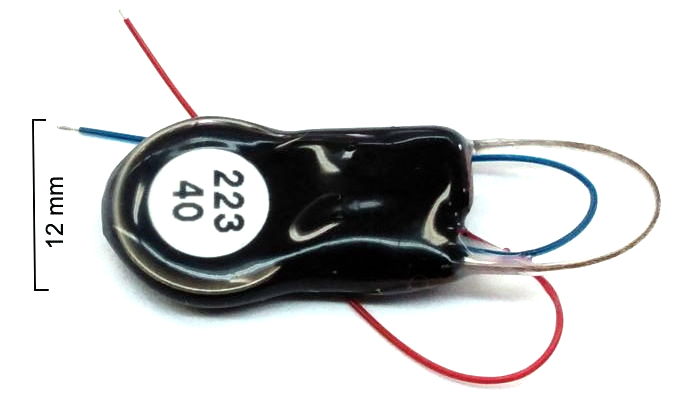
The A3048 amplifier can provide gain of ×100 for frequencies up to 160 Hz. The logic may be programmed to sample at 64, 128, 256, or 512 SPS. The low-pass filter may be configured for a corner frequency of 20 Hz, 40 Hz, 80 Hz, or 160 Hz. The input high-pass filter provides a corner frequency of 0.3 Hz, but may be removed to give gain all the way down to 0.0 Hz. All versions of the A3048 are equipped with 0.5-mm diameter red and blue leads, and a clear-coated loop antenna. The length of the leads, the battery loaded next to the circuit, the operating life, the termination of the leads, the sample rate, the gain of the amplifier, and the bandwidth of the amplifier all vary from one version to the next. The red lead is X+ and the blue lead is Xn−. The antenna is a 30-mm thin loop. The table below gives the specification of a particular transmitter version.
| Property | Specification |
|---|---|
| Volume | 0.89±0.1 ml |
| Mass | 1.8±0.1 g |
| Operating Life | 41 days |
| Battery Capacity | 2000 μA-days |
| Shelf Life | 6 months |
| On-Off Control | magnet |
| Lead Dimensions | diameter 0.5±0.1 mm, length 50±2 mm |
| Lead Terminations | steel coil, diameter 0.25 mm, length 1.0 mm |
| Number of Inputs | 1 |
| Input Impedance | 10 MΩ |
| Sample Rate | 256 SPS each channel |
| Bandwidth | 0.3-160 Hz |
| Noise | ≤8 μV rms |
| Distortion | <0.1% |
| Dynamic Range | 27 mV |
| Resolution | 16-bit |
| Absolute Maximum Input Voltage | ±3 V |
All versions of the A3048 are covered by a one-year warranty against corrosion and manufacturing defect.
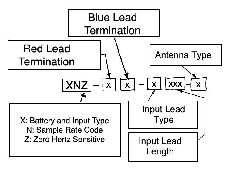
[02-FEB-24] The Subcutaneous Transmitter (A3048) can be equipped with a three, leads up to 130 mm, and a range of bandwidths, gains, and sample rates. You specify which transmitter you want with a full SCT part number. The part number begins with A2048 and is followed by the primary version letter that tells us the battery we load on the circuit. Following the letter we have one or two more numbers and letters that specify the sample rate of the inputs. We use the numbers 1-5 to indicate 128, 256, 512, 1014, and 2048 SPS respectively. We use the letter "Z" to indicate that the low end of the frequency response reaches all the way down to 0.0 Hz. After a dash we have a number and letter to specify the length and type of the leads. After a second dash we have letters specifying the electrodes, and after a final dash we have a letter specifying the antenna.
See our Electrode Catalog for a list of terminations and of depth electrodes to which our terminations can be attached. See our Flexible Leads table for a description of our several types of insulated, helical steel leads. See our Antennas table for a description of the various types of antenna we can deploy on our implants. The following versions are defined already, but we are happy to define new ones to suit your needs. The operating life is the minimum time for which a newly-made transmitter will operate continuously. The shelf life is the time the transmitter can remain turned off in storage and still retain 90% of its operating life.
| Version | Input | Battery Capacity (μA-dy) |
Volume (ml) |
Mass (g) |
Operating Life (dy) |
Shelf Life (mo) |
Status |
|---|---|---|---|---|---|---|---|
| A3048P0 | 0.2-20 Hz, 64 SPS, 27 mV | 1250 (CR1025) | 0.75 | 1.5 | 49 | 4 | Discontinued |
| A3048P1 | 0.2-40 Hz, 128 SPS, 27 mV | 1250 (CR1025) | 0.75 | 1.5 | 38 | 4 | Discontinued |
| A3048P2 | 0.2-80 Hz, 256 SPS, 27 mV | 1250 (CR1025) | 0.75 | 1.5 | 27 | 4 | Discontinued |
| A3048R0 | 0.2-20 Hz, 64 SPS, 27 mV | 1250 (CR1216) | 0.80 | 1.6 | 49 | 4 | New |
| A3048R1 | 0.2-40 Hz, 128 SPS, 27 mV | 1250 (CR1216) | 0.80 | 1.6 | 38 | 4 | New |
| A3048R2 | 0.2-80 Hz, 256 SPS, 27 mV | 1250 (CR1216) | 0.80 | 1.6 | 27 | 4 | New |
| A3048S0 | 0.2-20 Hz, 64 SPS, 27 mV | 2000 (CR1225) | 0.89 | 1.8 | 79 | 6 | Available |
| A3048S1 | 0.2-40 Hz, 128 SPS, 27 mV | 2000 (CR1225) | 0.89 | 1.8 | 61 | 6 | Available |
| A3048S2 | 0.2-80 Hz, 256 SPS, 27 mV | 2000 (CR1225) | 0.89 | 1.8 | 41 | 6 | Available |
| A3048S3 | 0.2-160 Hz, 512 SPS, 27 mV | 2000 (CR1225) | 0.89 | 1.8 | 25 | 6 | Available |
For input we specify the bandwidth, sample rate, input dynamic range, and channel number offset. In terms of ADC counts, the dynamic range is always 0-65535, as produced by a sixteen-bit ADC. The zero-value of an input is the sample we obtain when we short the two inputs together. The zero value depends upon the battery voltage, VBAT, according to Z = 1.8 V × 65535 ÷ VBAT. The dynamic range is the battery voltage divided by the gain of the amplifier. When we specify dynamic range, we assume VBAT = 2.7 V, which is true for most of the life of a lithium primary call. When the amplifier gain is 100, the dynamic range is 27 mV.
See below for details of current consumption and how to calculate battery life of new versions of the A3048. By default, we set the top of the frequency range at one third the sample rate. The A3048's low-pass filter provides 20 dB of attenuation at one half the sample rate. Frequencies above one half the sample rate will be distorted by sampling, and so compromise the fidelity of the recording. Because the EEG signal contains less and less power as frequency increases, this attenuation is sufficient to ensure that distortion is insignificant.
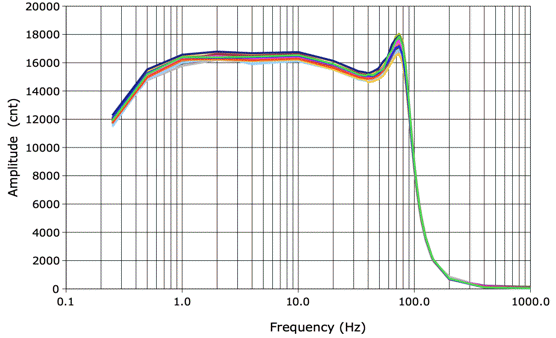
[26-FEB-24] The A3048 input usually consists of a 100-nF capacitor in series with a 10 MΩ resistor. These together form a high-pass filter with cut-off frequency 0.16 Hz. The A3048 amplifier provides gain of ×100, another high-pass filter, and a three-pole low-pass filter. We can remove the two high-pass filters by replacing the 100-nF input capacitor and another 10-μF capacitor in the amplifier with resistors. With no high-pass filter, the amplifier's pass-band extends down to 0.0 Hz. We configure the low-pass filter with corner frequency 20, 40, 80, 160, 320, or 620 Hz. These frequencies are matched with sampling rates 64, 128, 256, 512, 1024, and 2048 SPS respectively. The figure below shows the frequency response of twenty-two A3028S2 transmitters as recorded during Quality Control Two (QC2). You will find a database of such plots here.
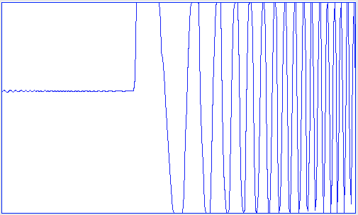
The amplifier is powered by the battery voltage, VB, which is typically 2.7 V, but will be 2.9 V for the first 5% of the battery's life and drop below 2.6 V in the final 5%. The amplifier saturates within 20 mV of 0V and VB. The following saturating sweep response shows how well the amplifiers handle large inputs. For a comparison of the A3048S2 saturation behavior and that of its predecessor the A3028S2, see here.
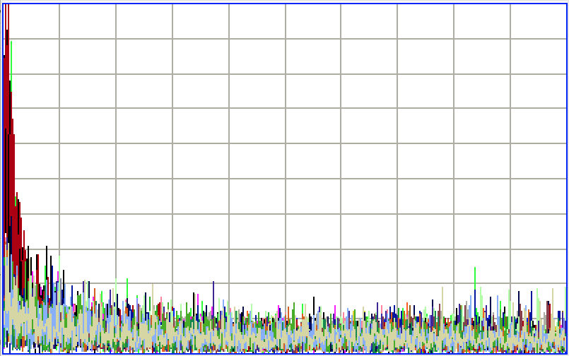
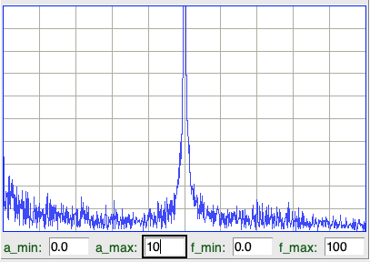
We measure the electrical noise on the A3048 input by placing the entire transmitter in water and letting it settle for a few minutes. Typical noise for an A3048S2 with 80-Hz bandwidth is 5 μV rms. The figure below shows the spectrum of electrical noise for a batch of A3048S2s.
The A3048P-series transmitters are equipped with a CR1025 coin cell. The CR1025 is 10-mm in diameter and 2.5 mm thick. When loaded with the CR1025, some transmitters will exhibit switching noise of amplitude up to 2 μV rms. This noise is caused by an interaction between transmitter's magnetic switch, which turns on and off at around 5 Hz, and the source impedance of the battery, which is larger for smaller batteries. Here is the electrical noise spectrum of a batch of A3048P2s.
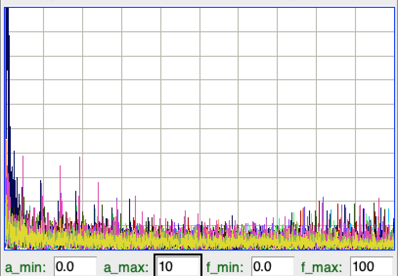
The switching noise we see in the A3048P-series transmitters consists of 10-ms pulses at roughly 5 Hz. The height of these pulses decreases with temperature. At 37°C, they will be no more than 10 μVpp, but at room temperature they can be as large as 30 μVpp. A typical EEG signal from a bare wire electrode in a mouse is 40 μV rms, 160 μVpp. Switching noise pulses of 10-μV are hard to see.
The distortion of a signal by our telemetry system is the extent to which it changes the shape of a signal. We apply a sinusoid to the X inputs of an A3048AV1. The AV1 is equipped with a 0.5-80 Hz amplifier with gain ×100. Input dynamic range is 27 mV. We increase the frequency from 1/8 Hz to 100 Hz. For each frequency, we obtain the spectrum of the signal and measure the power outside the sinusoidal frequency as a fraction of the sinusoidal power using this script. We express the result in parts per million.
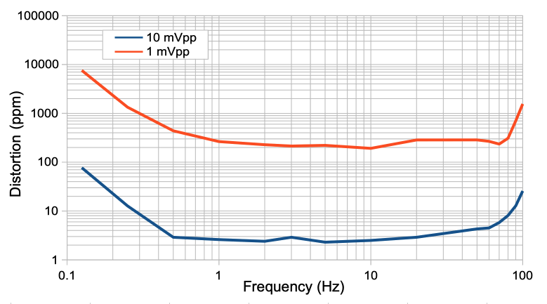
The distortion of X is dominated by random electronic noise. There are no significant peaks in the spectrum outside the fundamental.
The distortion generated by the A3048 is hundreds of time less powerful than that of its predecessor, the A3028P and A3028S. The A3048 samples the signal uniformly, thus eliminating the scatter noise present in the A3028 signal.
Details of the design are available in the following library of design files. Note that all our designs are protected by the GNU General Public Lisence.
S3048A_1.gif: Schematic of A3048AV1.The A3048AV1 circuit comes with a programming extension that provides the programming connector, a power plug, and test pins. The extension is connected to the SCT circuit by a 2.6-mm wide, 10-mm long neck. We use the extension as a way to hold the SCT during encapsulation. At some point during encapsulation, we clip the neck, leaving the SCT circuit on its own.

[20-JUL-23] The following table lists versions of the assembled A3049 electronic circuit, out of which we make the A3049-series transmitters.
| Version | Description |
|---|---|
| A3048AV1 | 0.5-80Hz, U5=MAX4471, L1=2n0, C6=OC |
| A3048BV1 | 0.2-80Hz, U5=OPA2369, C12=C13=15pF, R14=200R |
The BV1 is equipped with an effective antenna protection network, is equipped with an op-amp with maximum offset 0.2 mV, and has the gain of the amplifier spread between the two op-amps.
[04-AUG-23] Here we list the electronic circuits we can use to assemble the various types of A3049 transmitter, and the modifications required by that circuit prior to assembly.
| Transmitter Type | Circuit Version | C7 | C8 | C9, C10, C11 | R6 |
|---|---|---|---|---|---|
| 0.2-40 Hz, 27 mV | A3048BV1 | same | same | 3.9 nF | same |
| 0.2-80 Hz, 27 mV | A3048BV1 | same | same | same | same |
| 0.2-160 Hz, 27 mV | A3048BV1 | same | same | 1.0 nF | same |
The A3048BV1 produced by build B119305 have R3 loaded with 100 kΩ instead of 4.02 kΩ, so all these boards must be modified before calibration. At time of writing, we have 200 on the shelf. The next batch will have this error corrected.
[19-DEC-22] When we want to mark in our SCT recordings the time at which some event took place, such as the start of a video recording, the moment that a light was flashed, or when an noise commenced, we can use an auxiliary SCT to record a synchronizing signal along with the signals received from implanted SCTs. See the Synchronization section of the A3028 manual for details.
[29-APR-24] We equip all our subcutaneous transmitters with CR-series lithium primary cells. The voltage produced by these batteries begins at around 3.2 V, drops rapidly to 3.0 V, remains around 2.9 V for most of the battery's life, and drops rapidly towards the end of life.

The inactive current consumption of the A3048, which is its current consumption when it is turned off, is roughly 0.8 μA at room temperature. When we calculate shelf life, however, we use 1.0 μA for the inactive current consumption, so as to arrive at a conservative estimate of the time it will take for the A3048 to use 10% of its battery while sitting on the shelf. The CR1225 battery has capacity 50 mAhr ≈ 2000 μAdy, so its shelf life is 200 dy = 7 mo.

To obtain the operating life of an A3048 transmitter, we divide the battery capacity in μA-days by the maximum current consumption in μA, and then subtract one day. The subtraction of one day accounts for extended tests we perform during quality control. To obtain the maximum current consumption of an A3048 transmitter, we use the following relation.
We have 18 μA (eighteen microamps) base current consumption, which powers the logic chip (15 μA), amplifiers (1 μA), and miscellaneous circuits (2 μA). Additional current consumption for sample transmission is 0.11 μA/SPS (microamps per sample per second), or we could say that each sample requires 0.11 μC of charge from the battery. The above formula predicts 46 μA at 256 SPS. The formula above is the maximum current consumption of an SCT in order to pass our quality control tests. The average current consumption of the A3048 circuits is roughly 5% lower than the maximum.
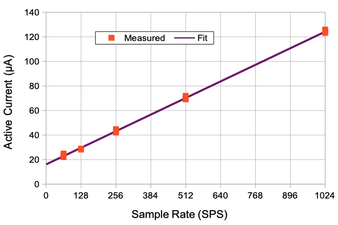
In the table below, we use our formula for maximum current consumption and combine it with the nominal capacity of the batteries we might use with the A3048. The CR1025 is the smallest CR-series coin cell available. The CR1620 is the largest coin cell we can load onto the A3048.
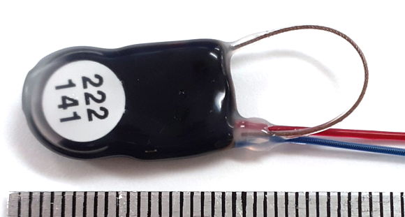
[29-NOV-23] All versions of the A3048 are encapsulated in black epoxy and coated with silicone. The silicone is "unrestricted medical grade" MED-6607, meaning it is approved for implants of unlimited duration in any animal, humans included. The A3048's leads and antenna are encapsulated with dyed silicone, then coated with the same unrestricted medical grade silicone. The only materials the transmitter and its leads present to the subject animal's body are either unrestricted medical grade silicone or stainless steel.
[30-MAR-23] Start circuit design.
[06-APR-23] We remove the low-pass filter that lies between VD and VA on an A3047A1A. That is: we remove R1 and replace with 0 Ω, leaving the 10-μF capacitor in place on VA. We see no increase in noise, no switching noise. The logic on the A3047 uses only 1V8. The only things using VD and VA are the VCO and the amplifiers. We resolve to remove this resistor from the A3048. We start with A3028PV3 circuit, replace LTC1865L with ADS8600. We now have enough free space to add a two-component antenna matching network. We are unable to fit two SC-353 single op-amps on the board. We must stick with the SOT-23-8 dual op-amp. We cannot purchase the OPA2349. The MAX4471 is available. It is a drop-in replacement with the advantage that it is rail-to-rail input and output, its input offset is only 0.5 mV, and its quiescent current is slightly lower. But its gain-bandwidth is only 9 kHz compared to the OPA2349's 70 kHz. But the only pup transmitters we have been making are 0.3-40 Hz and 0.3-80 Hz. The first amplifier has a gain of 40, so we need 3.2 kHz gain-bandwidth product. The MAX4471 will do the job easily, and will do okay with 160 Hz as well. We rotate the VCO so we can add our matching network. The RF signal propagates diagonally across the circuit board. We exchange the power and ground planes for two additional signal planes, making six signal copper planes in all. Re-name components so they are contiguous.
[08-APR-23] Layout A304801A complete, schematic S3048_1.gif.
[11-APR-23] Printed circuit board submitted for fabrication.
[14-APR-23] Panel Gerber files received. Note that logic chip LC4064ZE-7MN64I now in-stock at DigiKey.
[09-MAY-23] Receive 100 of A3048AV1. These are equipped with 2-nF capacitors for 80-Hz bandwidth, and resistors for ×100 gain. After correcting one constraint error in the code, the circuit works perfectly. It does have an , with the one idiosyncracy: when we power it on through our multimeter set to microamps or milliamps, the resistance of the meter causes the circuit to become stuck in a state where it consumes several milliamps and does not complete its turn-on. When powered by a battery, the circuit always turns on and off correctly. We program and test three circuits at 128 SPS, 256 SPS, and 512 SPS and find the average current consumption is 29, 42, and 69 μA respectively, which is 10% lower than the consumption of the A3028KV2. We compare the saturation behavior of the A3040D2 amplifiers, which are identical to the A3028S2 amplifiers, to that of the A3048S2.

[12-MAY-23] The A3041AV1 amplfier is equipped with a three-pole low-pass filter and MAX4471 9-kHz dual op-amp. If we remove this filter, we see the maximum bandwidth the amplifier can deliver. With 1.0 nF capacitors, the amplifier has a corner frequency of 160 Hz, and with 2.0 nF capacitors the corner frequency is 80 Hz. The AV1 assembly comes with 2.0 nF capacitors by default.

The A3048AV1 can provide a gain of ×100 with corner frequencies of 40 Hz, 80 Hz, and 160 Hz, but no higher. Its amplifier is not fast enough to provide a gain of ×100 at 320 Hz. The A3048BV1 will provide a faster amplifier.
[06-JUN-23] We add another passive component to the A304801A to make a T-network between the VCO and the antenna. We convert the amplifier to provide gain ×21 in first stage and x5 in second stage, for total of x105, as we did in A3049. The OPA2369, with its 12-kHz gain-bandwidth product, will provide gain ×21 up to roughly 500 Hz, while at the same time guaranteeing offset less than 0.75 mV, making the circuit suitable for amplifying biopotentials down to 0.0 Hz. We make some other adjustments to tracks and silk screen, generating A304801BR1, which we submit for fabrication, and new schematic S3048B_1. Assembly BV1 will be equipped with T-network C12=C13=15pF and R14=200Ω. This network gives complete protection against sparks from our plasma ball. It attenuates the transmit power no more than 1 dB. The BV1 will be loaded with 2.0-nF filter capacitors for 80-Hz corner frequency.
[28-JUN-23] We have two A3048S2 that failed in the same way during poaching, each after roughly twenty days. Prior to failure, sweep response is perfect every day. On the day of failure, the device won't turn on. Dissect both. Battery voltage is 1.5 V until we disconnect, then rises to 2.7 V. Connect battery to circuit, voltage drops to 1.5 V again. Jump start by connecting 2.7 V across battery briefly. Circuit powers up and transmits. Disconnect from battery. Connect external 2.7 V. Ater initial burst of current to power up the circuit, current consumption is ≈40 μA. Connect 10 kΩ to battery, voltage drops to 1.5 V. Connect 10 kΩ to fresh battery, voltage remains 3.22 V. If we connect either battery to an A3028KV2 circuit, one that consumes 75 μA, the battery can turn on the circuit, and battery voltage is around 1.9 V.
In a batch of 23 A3048P2, equipped with CR1025 battery, we see switching noise up to 2 μV rms, which consists of pulses of around 20 ms and height up to 30 μV at room temperature. For spectrum see here. We see no sign of such noise in the A3048S2 equipped with the CR1225 battery.
[30-JUN-23] Receive 120 of A3048AV1. Measure current consumption versus sample rate, add to our existing measurements, slope 0.106 μA/SPS, intercept 16.1 μA.
[19-JUL-23] Firmware P3048A05 provides uniform sampling with transmission scatter. The uniform sampling is achieved by always sampling at the end of each sample period, by asserting CSS for one CK period. The active CK period, when we read out the sample, takes place 1 to 16 CK periods later. We assert CSS only during the ADC readout, not for the full CK period. Applied to an AV1 assembly at 256 SPS we have current consumption 43.1 μA with scattered sampling and transmission. We have 43.4 with uniform sampling and scattered transmission. Distortion at 50 Hz drops from 40,000 ppm to 4.3 ppm.
[01-AUG-23] We have 200 of A3048BV1. First problem we discover is we specified 100 kΩ for R3. We must swap for 4.02 kΩ on all boards.
[18-AUG-23] We check the RF power emitted by the A3048AV1, with no antenna protection network, and the A3048BV1, with three-component T-protection network. Nathan reports. "We measured the RF power output of the A3048BV1 and compared it to that of the A3048AV1. We programmed and calibrated both boards. We then placed each one separately in a faraday enclosure and measured its power output using the spectrometer tool. They had comparable power output. We then tested its static protection by shocking the antenna of the transmitter with a spark from a plasma ball with a washer on top. The A3048BV1 survived the shocks from the plasma ball and operated perfectly fine afterward. The 3048AV1 lacked protection and would stop working after a couple sparks. The VCO would need to be replaced, indicated by the 18mA current consumption."
[02-OCT-23] We have our first batch of A3048 transmitters made with the A3048BV1 circuit. They are a batch of A3048S2-AA-C50-D. Noise in 1-80 Hz is 2-3 μV rms, a new record low for a batch of transmitters.
[31-JAN-24] In a batch of 24 A3048P2 transmitters, after one-day soak, we find that we have to turn each one on three times if we are to be certain that the circuit powers up correctly. When it powers up incorrectly, the signal reports value zero always. After QC2, we turn them all off, wait a few minutes, and turn each one on again with one touch of the magnet, every one of them powers up correctly. We are leaving them to soak for another few days, but this incident alarms us enough to discontinue use of the CR1025 battery and replace it with the CR1216, which has the same capacity, volume, and mass, but is provided by Murata with guaranteed pulsed current performance. The CR1216 by Murata can provide 10 mA for 10 ms in starting an A3041 IST. It can certainly provide 2 mA for 1 ms to power up an SCT. We choose version letter "R" for the new line of transmitters.
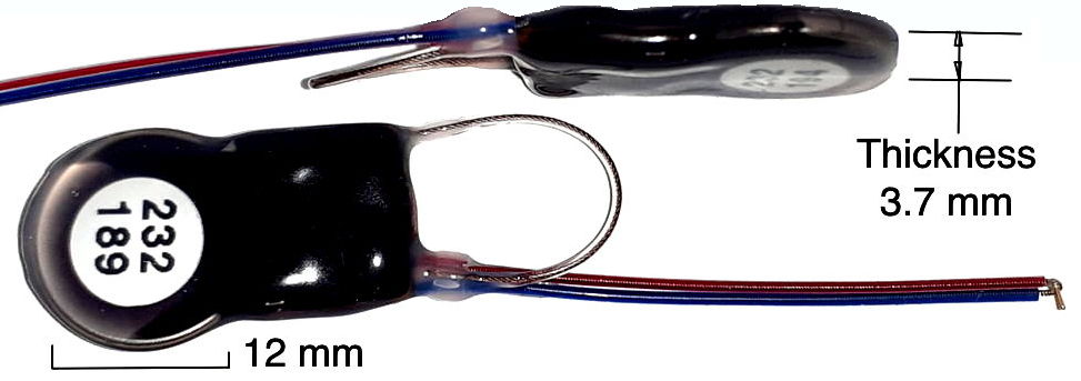
[09-FEB-24] We have our first batch of 24 A3048R2s passed through QC2, frequency response here. Mass is 1.67 g (nominal is 1.6 g), volume is 0.84 ml (nominal is 0.80 ml). The battery is as thin as the circuit board after encapsulation, see here.
[22-MAR-24] We measure current consumption for falling and rising battery voltage.

Nathan reports, "We measure the current consumption of an A3048S2 transmitter with respect to its battery voltage. First, we start by applying 3V and decreasing the voltage down to zero while measuring current consumption and notice that the device stops transmitting around 1.8V. Then, we start at 0V and increase the voltage applied on the circuit to 3V noting that the device begins to transmit around 2V." We note that this behavior will cause the transmitter to drain its battery if the power supply rises too slowly, or if it drops slowly. Slow drops are likely at the onset of corrosion in implanted transmitters, and we see such sudden drains in our poaching transmitters.
[25-MAR-24] During QC2 we find that No81 from a batch of A3049J2-AAAA-C45-D turns on for the first time and latches up: signals are both stuck at 65535. Turn off, turn on and it works fine. Turn off and wait ten minutes, turn on again, it latches up. We can get it to latch up or down (stuck at zero). We dissect. Current consumption is normal. We load the Renata CR1225 battery with 5 kΩ and observe source resistance 500 Ω. We load a fresh Renata CR1225 battery with 5 kΩ for a few hours, its source resistance is 100 Ω. We observed when choosing batteries for our ISTS that some Renata batteries have lower source resistance than others. The Renata batteries have no specified behavior for pulsed currents.
[04-APR-24] We have an A3048S2, S234.62, that generated 40 μV, 4-Hz spikes during QC2, this being switching noise from the magnetic sensor. We poached it. It failed 36 days, a few days short of its nominal 41-day operating life. We take this device and use it to investigate the relationship between battery source resistance and switching noise amplitude. Nathan reports. "Attached is an image of my setup for performing an experiment to measure the switching noise in relation to the source resistance in series with a CR2330 battery as the power supply. We increase the source resistance on the battery by adjusting a potentiometer and measuring its resistance each time. We then take a recording and play it back in the neuroplayer to view the fourier transform of the transmitter signal. Measuring the amplitude of the switching noise and its harmonics allows us to plot a relationship. See plot attached as well."

Switching noise harmonic amplitude, as seen in its spectrum, increases linearly with the resistor we insert between the battery and the transmitter.

Above 150 Ω the device latches up when we turn it on. Above 400 Ω it will not turn on at all. In order to obtain our measurements above 150 Ω, we start the circuit with a low-impedance source.
[10-APR-24] We find that the A3048, as well as the A3049, consumes 7 mA for 5 ms at startup, followed by 3 mA for 120 ms, when supplied through a 100-Ω resistor. The first rush is current flowing into the decoupling capacitors. The second is consumed by the ADS8860.
[16-APR-24] In March, we received S208.5 back from ION. It failed suddenly while implanted. We dissect and find VB = 2.9 V. In the recording of the moment of failure, X jumps 1 mV, then the transmitter turns off. We see the same failure in S237.102 after five days poaching. Nathan reports, "The signal from the transmitter looks like a saw tooth and its current consumption changes with small movements. To investigate this issue, we dissect. The battery voltage appeared normal at about 2.9 V both loaded and unloaded but the current consumption (only when on) was 200 μA higher than expected. This measurement did not decrease with applying 4.2 V to Vbat nor did it change when I heated the circuit. The current consumption didn't change much when I took off the VCO (U6); it only changed when I removed the ADC. With that in mind I dissected the transmitter that came back to us from Amy and replace its ADC. Once its ADC is replaced, the transmitter behaves normally."
When these two circuits were exhibiting their failure, touching the antenna or body lightly would improve reception for a moment, thus making it possible for us to see the saw-tooth provided by the signal. We see no way a faulty ADC could compromise reception. These transmitters both use the P3048A03 firmware, which latches SDO on the rising edge of TCK. Regardless of what the ADC does, there is no way for the transmitted bit stream to deviate from the format provided by the TXS state machine. For the ADC to compromise reception it must be dropping the VA power supply by consuming excessive current. When we do see reception, the ID is correct and present, but the ADC output appeasr to be either $8000, $0000, or $FFFF.
We wonder if firmware glitches could cause the ADC to misbehave. We note that SCK and CSS are partly combinatorial in the P3048A03 firmwarwe. We prepare and test firmware P3048A04, in which SCK and CSS are generated synchronously with TCK and CK.


We check frequency response (correct), noise (22 cnt rms), and distortion (<20 ppm). Current consumption at 64 SPS is 23.0 μA, at 256 SPS is 43.8 μA, and at 2048 SPS is 243 μA. Slope is 0.11 μA/SPS. Intercept 16 μA.
[29-APR-24] As we report here, the CR1225 from Multicomp provides far superior pulsed-current performance to the Renata CR1225, as well as what appears to be 50 mAhr capacity. We stop use of the Renata battery and start using the Multicomp.
[03-MAY-24] We have a batch of 14 of A3048S2 made with Multicomp CR1225. Noise is ≤2.5 μV rms, a new record. No trace of switching noise. The irregular pulses of around ten or twenty microvolts that we have been seeing in the S2 made with the Renata CR1225 are not present.