| Design |
| Modifications |
| Development |
[25-SEP-25] The A3025 H-BCAM Head introduced the first dual-ICX424AL camera. We discuss the behavior of the clock signals for the dual-sensor drive, in particular for quadruple-pixel readout, in this study.
[05-JAN-16] The A3025A H-BCAM Head requires no modifications. The A3025B requires a piece of kapton tape over the via that connects U1-2 through the board beneath J1. Without this tape, the via makes contact with the J1 shield.
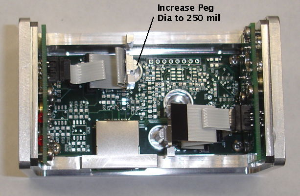
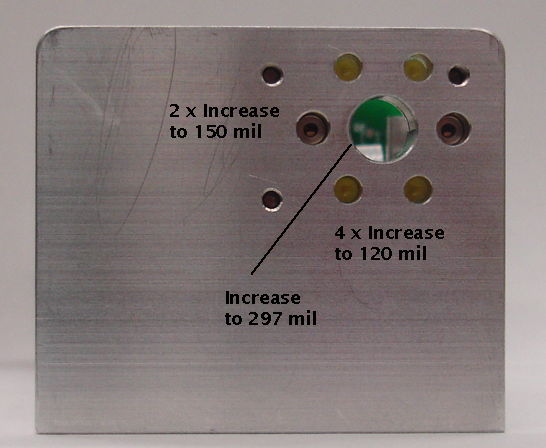
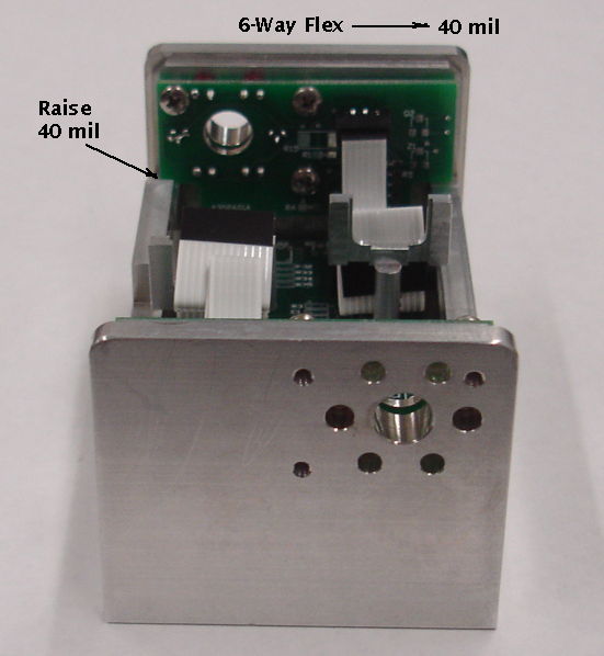
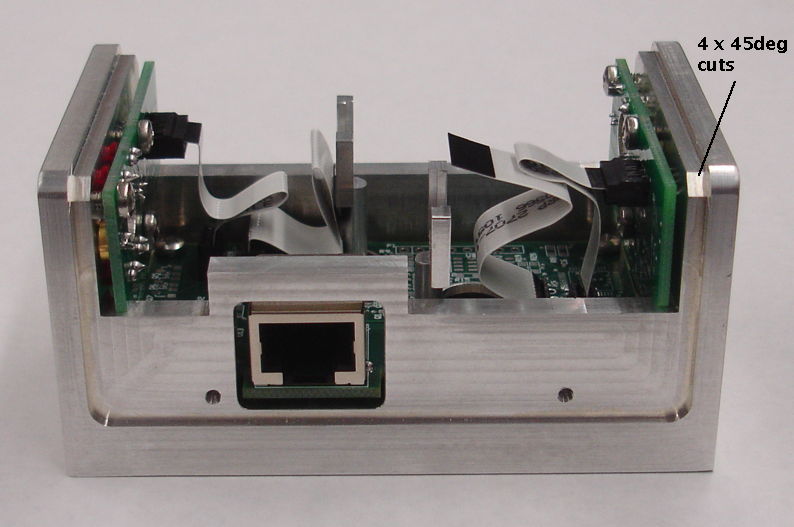
[09-JAN-13] We have the A302501A (Black H-BCAM main board), A302601A (Black H-BCAM side board), and a prototype chassis, not anodized, with two sensor mounting pegs. We assemble them together to test the mechanical fit. See H-BCAM, Top View for photograph. The flex cables must be bent several times, but they fit in the available space. See H-BCAM, End View for photograph. The lower mounting screw of the A302601A end board requires that we go through the opposite lens hole with the screwdriver shaft. We put up with this in the Polar BCAMs, so we can tolerate it in this design too. Once the pegs are in place, however, we cannot undo the lower screw, even if we remove the lens. This we will tolerate also. See H-BCAM, Top Angle View and See H-BCAM, Side View for photographs. We recommend the following changes.
[14-JAN-13] We assemble one A302501A printed circuit board. We have difficulty with solder bridges between vias and pads, especially when the vias are obscured beneath P0805 components. But the board works with both image sensors and appears to switch its source control pins to 0V.
[01-MAR-13] We now have four working A3025As.
[04-MAR-13] We discover that the A302501A layout has J2 and J3 in the wrong place, when compared to our original schematic, which was based upon the arrangement to be found in the Polar BCAM Head (A2051L). J2 was at the front of the board, when it should have been at the back for use in the front-facing camera. This problem can be fixed in the firmware, so we produce P2074A05, in which the CCD1 signal becomes CCD2, and we modify page three of the schematic to match.
[25-MAR-13] We have two fully-functional BCAM-HLDs, loaded with 7-mW lasers set to emit 5.5±0.5 mW. Because the laser power exceeds 5 mW, we apply Class 2M laser warning labels to the sides of the BCAMs. While testing these BCAMs we notice that a light source jut above the field of view of the rear-facing camera will shine light through the lens to the top surface of the RJ-45 connector, which is shiny metal. The result is light shining onto the image sensor from a light source outside its field of view. We were able to eliminate this reflection by placing a piece of tape on one side of the connector, protruding upwards, but not by applying nail polish. We will consider how to eliminate the reflection in future versions of the H-BCAM but for now we do not modify the BCAM to remove the reflection.
[27-MAR-13] The laser holes in the Blue H-BCAM chassis are making contact with the laser cans. We insulated the cans with kapton tape. In the future, we recommend increasing the diameter of the laser holes still further.
The spacers we are using for the side baords are 0.05" thick. We are doubling them up to make 0.10" spacing between the board and the chassis.
[02-APR-13] List of issues with the H-BCAM, including hardware. Overall, the new H-BCAM works well. It is accurate and all the circuits are correct and functiona. Here are some minor problems.
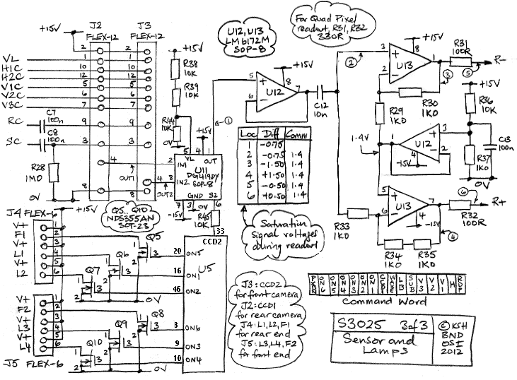
[06-AUG-13] We find that with 47-Ω resistors in place of R41, R42, R43 the H1 and H2 clocks are not formed properly in quadruple-pixel readout. This contrasts with the A2075, in which the clocks are formed properly. The A3025 loads the clock signals with two image sensors, and as a result the rise and fall time of the clock signals is longer. The 25-ns pulse required to double-clock the image sensor is attenuated. The image below shows the smearing of a BCAM image due to these poorly formed pulses in the A3025 quadruple-pixel readout.

We will solve this clocking problem in the future by replacing R41, R42, and R43 with 10-Ω resistors.
[03-SEP-13] The result of a study of double-speed clocking in the A3025 is here.
[25-SEP-13] We have an order for 56 H-BCAMs, half black and half blue. We resolve the issues listed on 02-APR-13 in the following way.
[06-JAN-15] We try various combinations of flex cables and image sensors in the two image sensor sockets, to see what kind of readout we can obtain.
| CCD1 (J2, Rear Camera) | CCD2 (J3, Front Camera) | CCD1 (Single) |
CCD1 (Quadruple) |
CCD2 (Single) |
CCD2 (Quadruple) |
|---|---|---|---|---|---|
| ICX424, 50-mm Cable | ICX424, 50-mm Cable | Perfect | Perfect | Perfect | Perfect |
| ICX424, 300-mm Cable | ICX424, 300-mm Cable | Perfect | Perfect | Perfect | Perfect |
| Omit | ICX424, 50-mm Cable | None | None | Perfect | Perfect |
| Omit | ICX424, 125-mm Cable | None | None | Perfect | Perfect |
| Omit | ICX424, 300-mm Cable | None | None | Bright pixels turn gray | Perfect |
| ICX424, 50-mm Cable | Omit | Very dim | Very dim | None | None |
| ICX424, 300-mm Cable | Omit | Very dim | Very dim | None | None |
These results show that the A3025 can operate with 300-mm flex cables, provided both image sensors are plugged in. If we want to load only one of the image sensors, it must be CCD2, but in that case the flex cable should be 125 mm or less.
As we can see, CCD2 must be loaded for CCD1 to be read out. When the A3025 wakes up to take part in a loop job, CCD2 is selected (see P2075A05.abl for firmware). The loop job measures the round-trip propagation time of the A3025's root and branch cables. If CCD2 is absent, input U11-8 to our image sensor selector switch floats to +15V, which sends a positive pulse through C12 to the output amplifier U13, resulting in a low pulse on R. The figure below shows the pulse on R− immediately after a wake command.
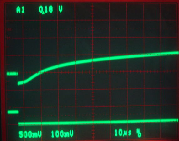
The low pulse on R corrupts the driver's measurement of loop time. The driver transmits a low pulse of its own, and is waiting for this pulse to return, but the low pulse generated by the wake-up arrives immediately, resulting in a 0-ns loop time measurement regardless of cable length. In future circuits, we will add a pull-down resistor to the image sensor outputs so that an absent image sensor does not cause pulses on R.
[30-DEC-15] We have an order for 12 Blue H-BCAMs. We have in hand 14 of the A3025B. We program them with firmware P2075A05. We capture images and flash all six light sources. The delay A to DA is 104 ns, and A to DDA is 230 ns. Ideally, these should be 125 ns and 250 ns (see specification). We adjust the firmware and get DA at 132 ns and DDA at 258 ns. We now have P3025A01.
[05-JAN-16] We have 14 A3025Bs with connectors loaded. We program and test with all sources and sensors. We add support for the A3025A/B to the Analyzer Tool. Current error for all boards is less than 5 mA.
[24-JAN-24] We update the Black H-BCAM main board layout, creating A302501C with smaller vias that we will have tented and masked. We delete the holes for CCD posts, since we have eliminated the posts. We space out the component designations so they are easy to read. We add 0V pad and power supply test points. Submit for fabrication.
[22-MAR-24] The new Black H-BCAM main board A302501C was far easier to work with than its predecessor. We build around twenty by hand for a PIPII order. We have four of the boards left, not panelized.
[17-JUL-25] We have an order for 36 of Black H-BCAM. We plan to have the main boards and side boards made by machine. Bill of materials is A3025AV2. All components are in stock at Digi-Key except the obsolete NDS356AP. We have plenty of these on the shelf, and will assemble the new boards with our old stock. The NDS355AP's radiation tolerance is well-known.
[23-JUL-25] One of our A3025AV1 assemblies, build on the A302501C board, produces a perfect image with a short cable, a dark image with a 3-m cable, and a negative image with a 5-m cable. The loop-back at the start of a new image, which measures the cable propagation time, is failing. We have seen this problem before but can find no report on it. We find that the R− line is corrupted during readout of bright pixels. We replace U1 and the problem resolves: we see bright images for all cable lengths. We resolve to add to our quality control a test of the cameras with short and long cables.
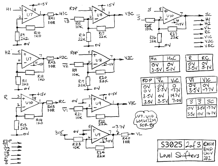
[15-SEP-25] We have forty A3025LV1 assemblies. Almost half of them fail Diagnostic Instrument loopback, returning either 0 ns or 3125 ns. We set up our test board and a faulty board, looking at R+ and R− during the loopback, to see what difference we can find.
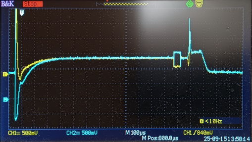
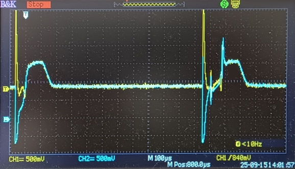
In the working board, we see the R+ and R− settling to 1.4 V, as dictated by U13 through 100-Ω resistors. We see the two lines separating by 0.5 V during loop-back, when we enable the LVDS driver and assert a HI on the return lines. When we examine the loop-back event in detail we see HI with a short LO period that marks the loop-back return. We check LB on both boards and it is being asserted in the same way. We check the A-DA and DA-DDA delays and find them to be about 125 ns, which is perfect. On the faulty board, the return lines settle to 1.0 V. It turns out that the board is not waking up. When we send command 0x0080 we see a 10-ns pulse on WAKE. When we send 0xFFFF, WAKE is asserted. We set each other DC (device command) bit to 1 in turn and find that with 0x00A0, which is DC6 and DC8 asserted, WAKE turns on. We get no WAKE with 0x0020. Bit DC6 is the substrate clock control. We have S = DC6 and !S = !DC6. We set S = 0, no change. We restore S = DC6 and set !S = 0. No change. We try another of the faulty boards and it exhibits the exact same symptom. We add another gate to the ring oscillator: no change. We set S = 1 and !S = 0, so that there is no change to these two lines as we wake the board, and they are always HI and LO. Now we can wake the board with 0x0080. Restore firmware. Load 10 nF across R27 to slow down the SC pulse. Still have failure to wake with 0x0080. The signal on S is a 20-V oscillation with period 10 ns. We remove R25. No change. Raise U10-7 off its pad. No change. Restore the SC amplifier. Set S and !S to 0 in firmware. Now cannot wake the board with 0x00A0. In the firmwarwe, we are back to our original code. We change run_time from dda_delay+3 to dda_delay+7 and now we cannot wake the board with 0x00A0. We drop to dda_delay+1 and behavior is same as for dda_delay+3. We change the code so that the ring oscillator is running all the time. We now get wake on 0x0080 and loop time that varies from 0 to 100 ns. The board consumes 8 mA from +5 V. Right now we are compiling our firmware P3025A02 for the LC4064ZC. But our new boards are equipped with the LC4064ZE. We can configure each output individually. We turn on pull-up resistors, set the outputs to slow-slew, and configure for 3.3-V I/O. We re-program our two faulty boards and now they wake up with 0x0080 and perform perfectly.