 A3050 Design
© 2024 Nathan Sayer, Open Source Instruments Inc.© 2024-25 Kevan Hashemi, Open Source Instruments Inc.
| Design |
| Modifications |
[19-SEP-25] All our designs are free and open-sourcde, copyright Open Source Instruments Inc, under the GPL 3.0 license. This circuit was designed by Nathan Sayer, but it is based upon the design of the A3031 Function Generator (A3031) by Michael Bradshaw.
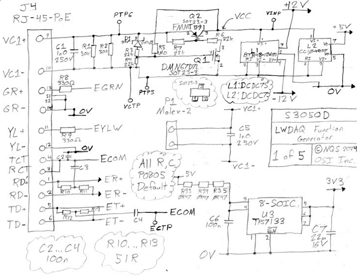
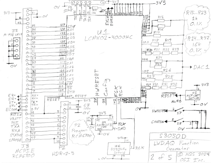
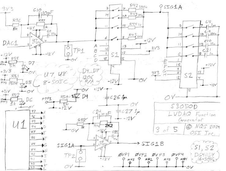
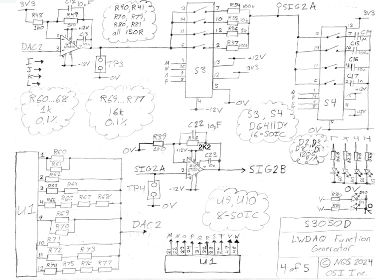
The generator logic runs off an 80-MHz clock. It divides this 80 MHz by two to obtain its 40-MHz waveform clock, which it then divides further by a user-programmable update divisor to generate the update frequency. The bytes read from the waveform memory drive the eight-bit DACs directly. The DACs produce 0-3.3 V. A level shifter takes the DAC output and turns it into −1.65 to +1.65 V. Amplifiers convert this range into ±10 V. After the final amplifier, we have a 50-Ω 3-W resistor, which makes the outputs tolerant of continuous short-circuits.
The signal itself will be made up of at least two sample values, and all these values will be written to the waveform memory during waveform configuration. Our LWFG routines always uses at least half of the 8-KByte memory by repeating the waveform as many times as necessary. By allowing itself to repeat the waveform, we are able to generate frequencies with precision better than ±0.1%.
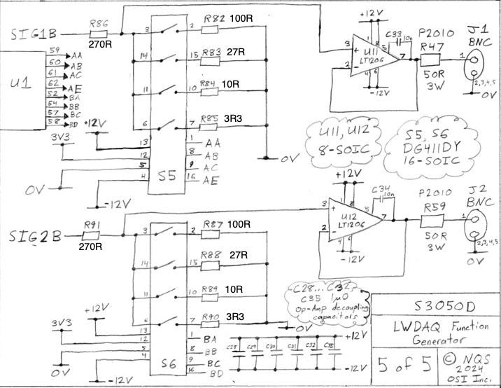
[21-NOV-24] To create the A3050C out of the A3050B, we load 270 Ω for the attenuator series resistors R86 and R91. We load divider resistors 100 Ω, 27 Ω, 10 Ω, and 3.3 Ω for both channels. We load 2.2 kΩ for R46 and R58 to increase the output amplitude.
[25-OCT-23] We receive new PCBs (A305001B) and assemble one. We notice that as soon as power is supplied, the +/-12V DC-DC converter begins buzzing. The logic chip can program so we now have a working extension, but we found that we must remove the feedback capacitors (10pf) on each op-amp in order to avoid drawing too much current. After removing these capacitors, we put a 3.3V 32.768kHz signal through both DAC channels and watch it propagate through the amplifiers. Each channel outputs a 10Vptp 32.768kHz signal with a 0V average.
[18-DEC-23] We program the controller (LCMXO2-7000HC) with a relay interface that maps various address spaces to variables needed to output a function. The data portal is located in the highest location in the control space.
[19-DEC-23] As an example waveform, consider a 10-Vpp, 1.25-MHz sine wave. We can do this by writing "128, 152, 176, 198, 218, 234, 245, 253, 255, 253, 245, 234, 218, 198, 176, 152, 128, 103, 79, 57, 37, 21, 10, 2, 0, 2, 10, 21, 37, 57, 79, 103" to the waveform memory. We write 31 to the waveform length and 0 to the divisor. We now have a sample clock of 40 MHz / 1 = 40 MHz, and we have 32 samples to step through, so we produce the entire waveform at 1.25 MHz.
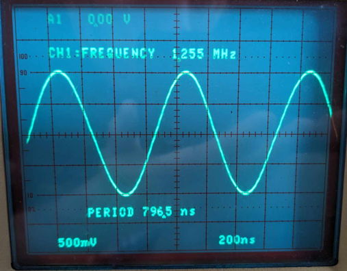
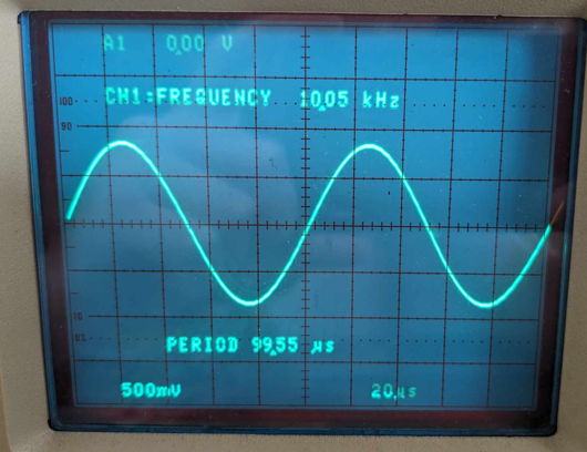
The 1.25 MHz sine wave was fast enough that it didn't require a filter to smooth out. We now write 124 to the divisor register and our frequency drops to 10 kHz.
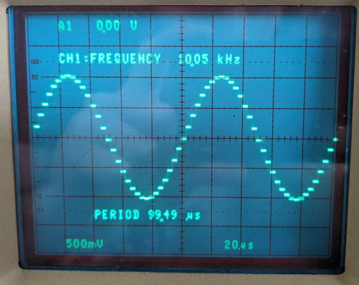
We can see each sample as a step in the sinusoid. We write "34" to the filter control register. The resulting waveform has about 1 dB less amplitude but looks smoother, as a result of the low-pass filter we deploy with our filter register.
The LWFG package picks the filter function automatically to suit the period of sinusoidal and triangle waves. It always disables the filter for square waves.
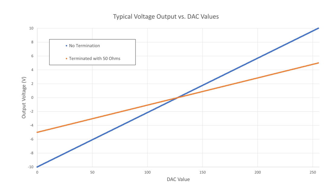
[03-JAN-24] The dynamic range of the generator outputs is ±10 V for a high-impedance load, or ±5 V for a 50-Ω load. The plot below shows how the output voltage varies with the signal value. Each signal value is an eight-bit number that drives the channel's digital to analog converter.
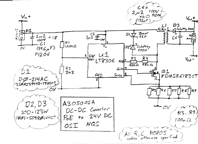
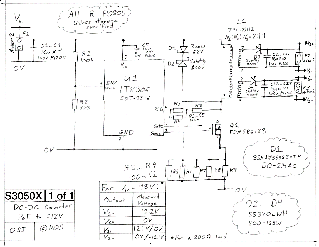
[24-JAN-24] To avoid supply shortage issues later on, we develop a DC-DC converter using the LT8306 no-opto isolated flyback converter. Using the LT8306 datasheet, we come to the following design:
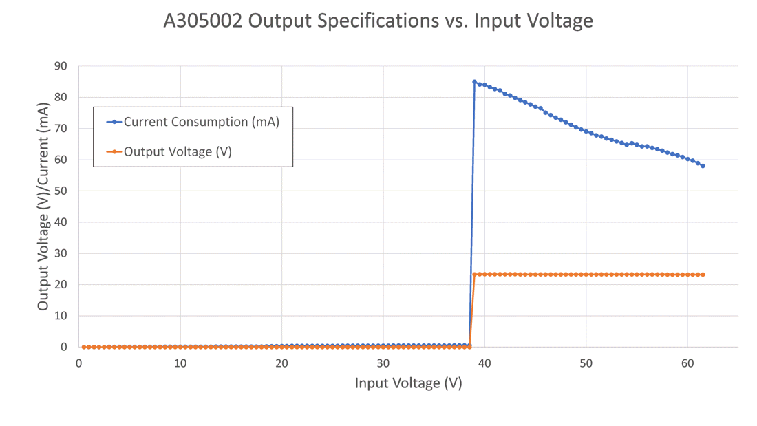
Once assembled, we test the converter by slowly ramping up its input voltage with a DC benchtop power supply and measuring its current consumption as well as its output voltage.
We then use these measured values to calculate the input power and output power. The efficiency measured in the graph below is defined as the output power divided by the input power.
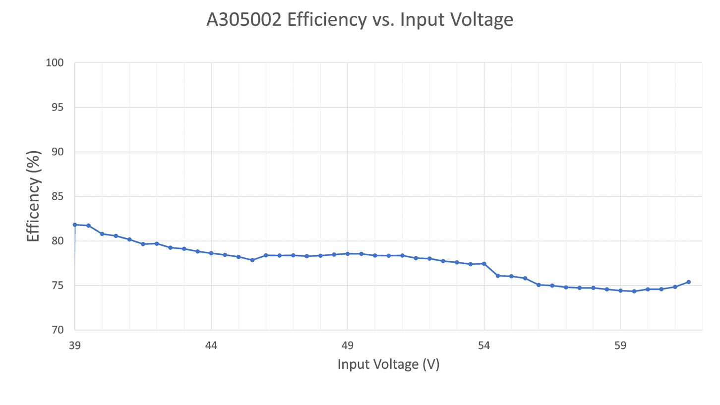
[29-JAN-24] We notice that with a 0.01 Ohm sense resistor the output voltage varies greatly based on input voltage. We increase the sense resistor to 0.025 Ohms and notice that the output voltage stabilizes with respect to input voltage.
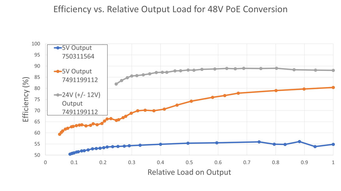
[07-MAY-24] We change the transformer used and attempt to output different voltages, measuring efficiency while increasing the output power.
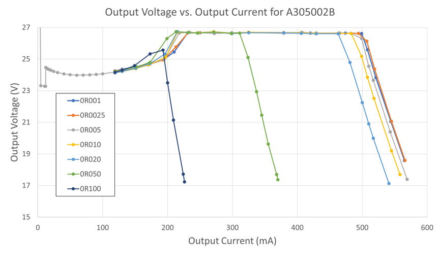
[17-APR-24] We get a new PCB for the DC-DC converter, A305002B and test. This new PCB allows us to choose between one output voltage and two differential output voltages by loading 0R resistors on some P0805 footprints. This allows us to use one PCB for different converters, versions below:
| Version | R6 Value | R7 Value | R8 Value | Output Voltage |
|---|---|---|---|---|
| A3050DC-S5 | OC | SC | SC | +5V |
| A3050DC-D5 | SC | OC | OC | ±5V |
| A3050DC-S12 | OC | SC | SC | +12V |
| A3050DC-D12 | SC | OC | OC | ±12V |
[17-APR-24] We assemble a converter in the ±12V configuration and plot its output voltage vs its output current for various values of R_sense. Results below:
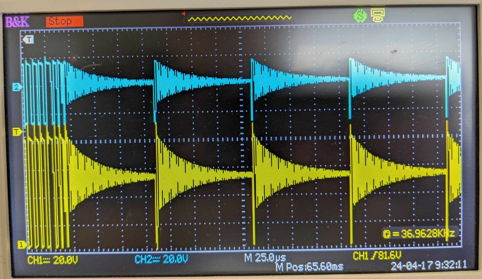
[18-APR-24] We measure the voltage at the drain of the MOSFET and the output of the transformer using an oscilloscope at various time divisions. Plots below.
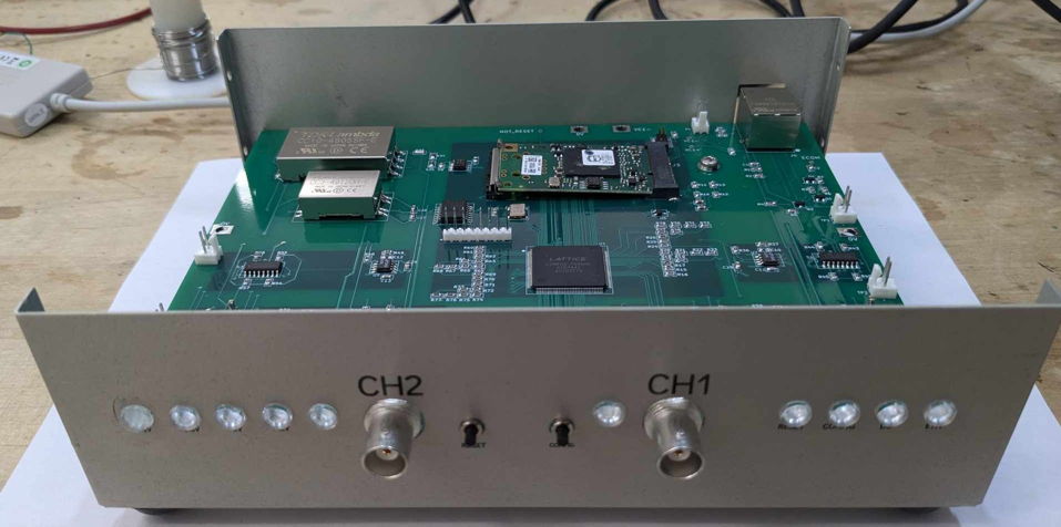
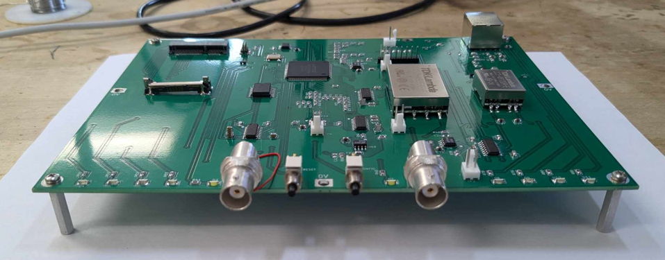
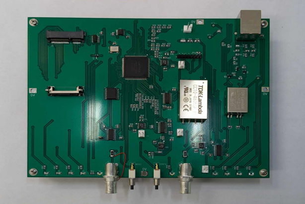
[06-JUN-24] We image the A3050A prototype for record keeping. This version does not include the attenuating switches before the output but still works otherwise.
[24-JUN-24] We construct a +5V PoE DC to DC converter and measure its output current and voltage with different values of R_Sense. Results Below.
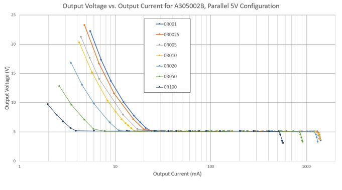
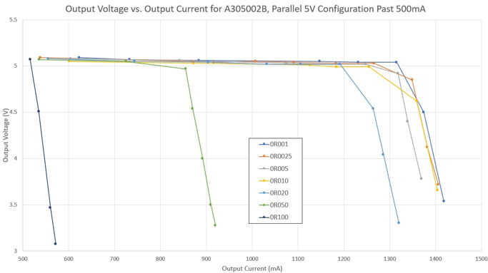
The 7491199112 PoE Wurth Electronik transformer that we use claims to have a 1.3A saturation current which is consistent with the end behavior of the lower valued R_Sense plots.
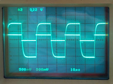
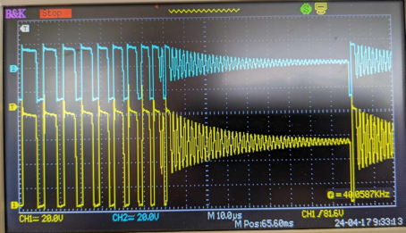
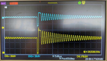
[03-NOV-24] Work on firmware V2. Remove 32.768 kHz clock input. Route control registers direct to output pins. Standardize names. Simplify sample clock generators. Re-arrange register memory map so registers for each channel are grouped together and separated from the registers of the next channel. Separate attenuation control for CH1 from CH2. Compile, test, all working, firmare V2.3 tagged. We note that the attenuators added to the circuit in the final S3050D version include a 2-kΩ series resistor that creates a 200-ns time constant with the 100-pF input capacitance of four analog switches, even when the switches are open.
[04-NOV-24] Load 270-Ω for R86 and R91, these are the series resistors of the two attenuators. Our 10-Vpp, 50-Ω terminated square wave now has 90% rise and fall times 200 ns. This time constant arises at the output of the eight-bit resistor DAC, where the 250-Ω source resistance of the DAC seems to be charging a 1-nF capacitor, although we do not know where that capacitor resides. The input capacitance of the LT1206 is supposed to be 2 pF. Our attenuator with 270-Ω resistor, solves the speed problem, but raises the significance of the 25-Ω typical resistance of the switch channels. We have divider resistors 100 Ω, 27 Ω, 10 Ω, and 3.3 Ω. We automate the selection of the attenuator in LWFG V1.7. We increase R46 and R58 from 2.0 kΩ to 2.2 kΩ to make sure we achieve the full ±10 V output range. We calibrate the five attenuator settings and arrive at the following pairs of attenuation and register codes for Channel One of Y71062, "1.04 0x00 0.320 0x01 0.116 0x03 0.0588 0x07 0.0360 0x0F". Thes values work to within ±1% on Channel Two as well.