| Design | |||||||
| Modifications | |||||||
| Demonstration Board | |||||||
| Development | |||||||
|
[19-MAR-26] All our designs are free and open-source, copyright Open Source Instruments Inc, and distributed under the the GPL3 license only, unless otherwise stated. In the case of the A3053 design, all files are GPL3-only, with the exception of the Demonstration Board Schematic, which we distribute in addition under the MIT License. The MIT License permits free use of the circuit in private designs, but provides no warranty.
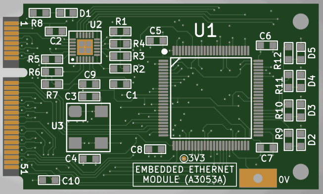
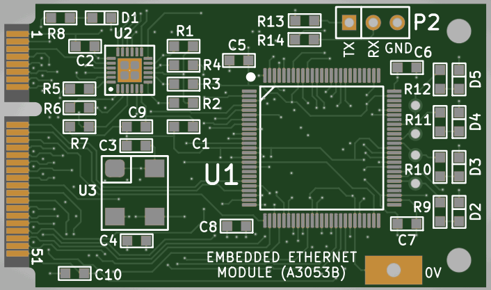
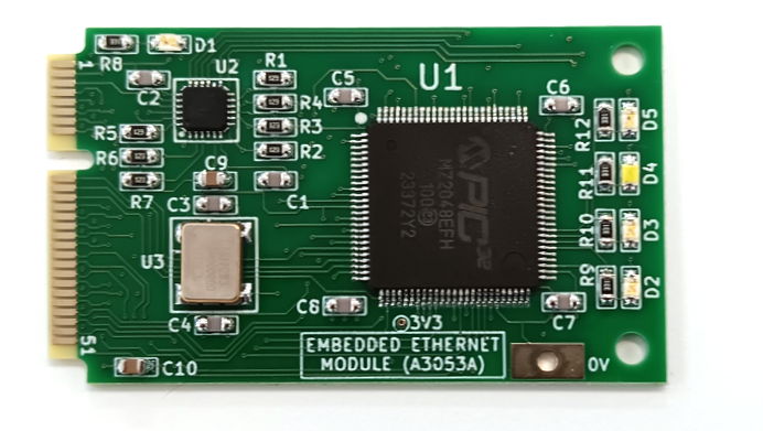
[22-NOV-25] To make the A3053A using the A305301A PCB we make the following hand modifications.
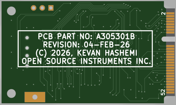
[06-FEB-26] Here are the modifications we made to the A305301A to create the A305301B.
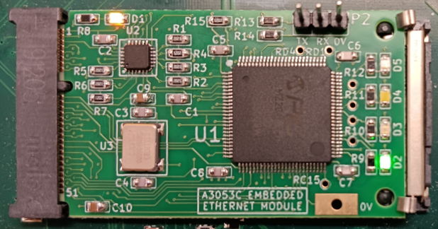
[11-MAY-26] Here are modifications made to the A305301B to create the A305301C.
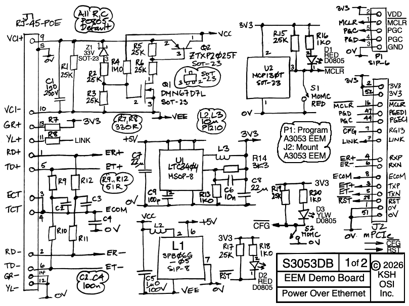
[01-JUL-26] We abandon plans to make a demonstration board for the A3053C Embedded Ethernet Module, but the A3053DB is already designed, so we preserve here our notes on the circuit, which are dated 23-MAR-26.
[23-MAR-26] In order to facilitate the adoption of the A3053 for use in new host boards, we are going to design and produce an A3053 Demonstration Board, part number A3053DM. This board will provide an mPCIe socket to accept an A3053 Embedded Ethernet Module, a programming plug, a PoE power detector, switch, and converter, an RJ-45 socket, and accompanying Ethernet signal balancing resistors and capacitors. This demonstration board will will offer under two licenses. The first license will be our default GPL3 license. The second license will be the more permissive MIT license. Our objective in offering the A3053DB design under the MIT license is to permit new users of the A3053 Embedded Ethernet Module to incorporate the PoE and network socket circuits onto their host boards without any requirement that the host board design be open-sourced.
[23-MAR-26] The purpoose of the A3053DM is to allow potential new users of the A3053 to try out compiling modified code for the module, programming the module, and testing its network connection. This demonstration board will be a rectangular circuit board with four standoffs so it will sit on your workbench. It will provide an mPCIe socket for an A3053 Embedded Ethernet Module. It will provide an RJ-45 socket with magnetics and associated resistors and capacitors to provide the A3053 with its wired network connection. There will be no separate power plug. Instead, the A3053DB will providea a Power-over-Ethernet (PoE) detector circuit and converters to provide 3.3 V for the A3053 using its network cable. In order to power up the A3053DB, connect it to a PoE switch. We will be distributing the design of the A3053DB under the MIT license, so you can incorporate the PoE circuits into your own proprietary circuit design if you wish. The A3053DB will provide some light-emitting diode (LED) lamps for the general-purpose input-output signals on the mPCIe socket, as well as some switches to set logic levels, and a through-hole breadboard area. A six-pin programming plug will allow you to program the A3053's PIC32MZ using a PICKit 5 programming adaptor.
[23-MAR-26] The design of the A3053DB Demonstration Board we offer under two licenses. We issue it under our usual GPL3, but also under the more permissive MIT license. Under the MIT license, you are permitted to include the A3053DM design in the design of your own host board. In particular, you are free to use the A3053DB's Power-over-Ethernet detector and switch circuit, as well as the resistors and capacitors around the Ethernet socket. Here is the MIT license statement for our A3053DB design files.
License for the A3053DB Demonstration Board

The A3053DB Demonstration Board hardware design, including its schematics,
printed circuit board layout, and related design documentation, is licensed
under the MIT License. The A3053DB design may be used in proprietary systems
without requiring those systems to be open-sourced. This license applies only to
the A3053DB Demonstration Board design files. All other materials on this page
remain licensed under the GNU General Public License v3.0 (GPL-3.0) unless
otherwise noted.

Copyright (c) 2026 Open Source Instruments, Inc.

Permission is hereby granted, free of charge, to any person obtaining a copy of
this software and associated documentation files (the "Software"), to deal in
the Software without restriction, including without limitation the rights to
use, copy, modify, merge, publish, distribute, sublicense, and/or sell copies of
the Software, and to permit persons to whom the Software is furnished to do so,
subject to the following conditions:

The above copyright notice and this permission notice shall be included in all
copies or substantial portions of the Software.

THE SOFTWARE IS PROVIDED "AS IS", WITHOUT WARRANTY OF ANY KIND, EXPRESS OR
IMPLIED, INCLUDING BUT NOT LIMITED TO THE WARRANTIES OF MERCHANTABILITY, FITNESS
FOR A PARTICULAR PURPOSE AND NONINFRINGEMENT. IN NO EVENT SHALL THE AUTHORS OR
COPYRIGHT HOLDERS BE LIABLE FOR ANY CLAIM, DAMAGES OR OTHER LIABILITY, WHETHER
IN AN ACTION OF CONTRACT, TORT OR OTHERWISE, ARISING FROM, OUT OF OR IN
CONNECTION WITH THE SOFTWARE OR THE USE OR OTHER DEALINGS IN THE SOFTWARE.
[23-MAR-26] The A3053DB Demonstration Board is a Power-over-Ethernet (PoE) host board for an A3053 Embedded Ethernet Module that provides access to a selection of pins on the A3053's PIC32MZ2048EFH microcontroller. We communicate with the A3053 through the same network cable that provides power from a PoE switch. The schematic of the entire demonstration board we distribute under both GPL3 and MIT licenses, so you are free to use the PoE circuit in your own private host board design. You will find the demonstration board schematic in two pages S3053DB_1 and S3053DB_2.
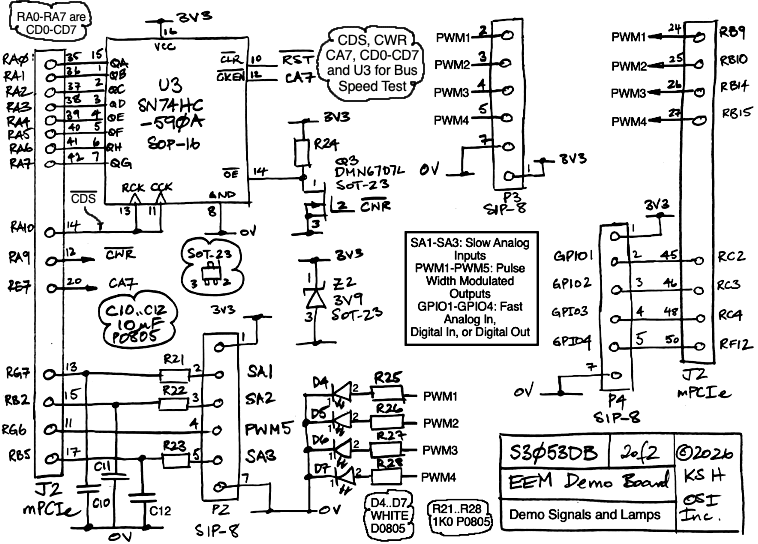
[23-MAR-26] The A3053DB Demonstration Board provides pulse-width-modulated (PWM) outputs PWM1-PWM4 on a SIP-8 header. These same signals are connected to four white light-emitting diodes (LEDs), so that the brightness of the LEDs will represent the modulation of the signals. The P3053 command-line interpreter (CLI) provides a command that configures these signals as PWM outputs and sets their modulation. When we compile the P3053 code for the A3053DB mother board, the main program will configure the four pins as PWM outputs and the main event loop will adjust the modulation so as to make a display on the white lights. A fifth PWM output, PWM5, is connected to another SIP-8 head along with three low-pass filtered analog inputs SA1-SA3. Each of SA1-SA3 pass through a 16-Hz low-pass filter before being presented to an analog input pin on the A3053's PIC32MZ. By jumpering PWM5 to SA2 or SA3 on the SIP-8, we can see the low-pass filtered PWM signal on an analog input. We can use CLI commands to configure the SA1-SA3 pins as analog inputs, and then read their values. A third SIP-8 provides four general-purpose input-output pins. These can be analog inputs, digital outputs, or digital inputs. They can be configured with CLI commands.
[23-MAR-26] To measure the speed of communication between the A3053 Embedded Ethernet Module and its host board, the A3053DB Demonstration Board provides an eight-bit counter whose output is connected to mPCIe parallel bus data lines CD0..CD7. This parallel bus is the one we ourselves use to communicate with our instrument host boards. The P3053 code provides all the routines we need to access this bus over the local area network. The mPCIe bus routines are in pic.h and the LWDAQ messaging protocol routines for the network side of the communication are in lwdaq.c. When we read from mPCIe bus locations 0x00 to 0x7F, the counter increments at the end of the cycle. If we read from 0x80 to 0xFF, the counter does not increment. When we perform a stream read from the bus, we will get an incrementing eight-bit value, which we can display as a gray-scale image 256 columns wide. If we stream read 65536 bytes, we will get a square image with a gray scale from left to right. If we are dropping bytes, or some values are being mis-read, there will be glitches in the gray-scale image. By putting scope probes on the A3053DB test points, we can see how fast the read is progressing. In addition to the SIP-8 connectors on the A3053DB Demonstration Board, the board also provides test points for CD0-CD7, !CWR, !CDS, CA7, the counter's !RCO carry output, and a selection of additional PIC32MZ pins. It provides a small through-hole breadboard area to assist with connecting external signals and breadboard circuits.
[04-AUG-25] Settle upon MCU and Ethernet PHY. In this HTML page we are trying out a Markdown renderer, which we may or may not employ in new entries. Examine the HTML source code for the markdown script and configuration. We use a dedicated "md" tag for the Markdown fields. If the browser fails to load the converter JavaScript, the HTML will instead replace the "md" with a "pre" field so we can still see the Markdown formatting.
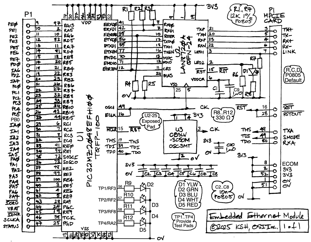
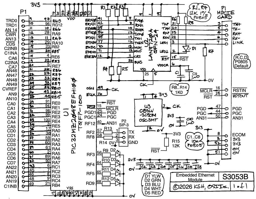
[08-AUG-25] We want the PIC32MZ in TQFP-100 to provide an RMII (Reduced Media Independent Interface), JTAG (four-wire programming of PIC32MZ), ISCP (two-wire programming of PIC32MZ), and an eight-bit external data buse (for communicating with the LWDAQ controller). We will have the PIC32MZ as U1 on the circuit, the LAN8720A Ethernet physical layer as U2, and the MPCIE connector as P1. Here are the required connections between U1 and U2 for the RMII.
| PIC32MZ Signal | U1 Pin | LAN8720A Signal | U2 Pin | Description |
|---|---|---|---|---|
| ERXD0 | U1-41 | RXD0/MODE0 | U2-8 | Receive Data 0 |
| ERXD1 | U1-42 | RXD1/MODE1 | U2-7 | Receive Data 1 |
| ERXERR | U1-35 | RXER | U2-10 | Receive Error Input |
| ETXD0 | U1-86 | TXD0 | U2-17 | Transmit Data 0 |
| ETXD1 | U1-85 | TXD1 | U2-18 | Transmit Data 1 |
| ETXEN | U1-77 | TXEN | U2-16 | Transmit Enable |
| EMDC | U1-70 | MDC | U2-13 | Management Data Clock |
| EMDIO | U1-71 | MDIO | U2-12 | Management Data |
| EREFCLK | U1-16 | REFCLKO | U2-14 | Reference Clock Out |
| ECRSDV | U1-12 | CRS_DV/MODE2 | U2-11 | Carrier Sense Data Valid |
The LAN8720A requires !RESET on its nRST input, U2-15, which arrives on the board through mPCIe pin P1-16. There are various ways to provide a clock for the synchronous RMII bus. We will load a single 50-MHz oscillator on our board and drive three inputs with the oscillator signal directly: U1-16, U1-49, and U2-5. These are the EREFCLK and OSC1 inputs of the PIC32MZ, and the XTAL1 input of the LAN8720A. We leave U2-4 floating. We route unused, multi-purpose GPIOs from the PIC32MZ to all the connections on the mPCIe connector that have a signal function on the RCM6700. For the six programming connections, we give the programming bus name and the short signal name. These signals are PGC and PGC for the ICSP bus and TCK, TMS, TDI, and TDO for the JTAG bus.
| A3053A Signal | RCM6700 Signal | mPCIe Pin |
|---|---|---|
| 0V | GND | P1-1 |
| +3V3 | +3.3 V | P1-2 |
| U2-21, TXP | Tx+ | P1-3 |
| U2-23, RXP | Rx+ | P1-4 |
| U2-20, TXN | Tx− | P1-5 |
| U2-22, RXN | Rx− | P1-6 |
| U2-3, LINK | LNK | P1-7 |
| ECOM | ECOM | P1-8 |
| U1-97, RG13 | PE0 | P1-9 |
| U1-2, RA5 | PE1 | P1-10 |
| U1-10, RG6 | PE2 | P1-11 |
| U1-82, RD5 | PE3 | P1-12 |
| U1-11, RG7 | PE5 | P1-13 |
| U1-81, RD4 | PE6 | P1-14 |
| U1-18, RE8 | PE7 | P1-15 |
| U1-15, !MCLR | !RESET_IN | P1-16 |
| U1-20, RB5 | PD0 | P1-17 |
| U1-21, RB4 | PD1/IA6 | P1-18 |
| U1-22, RB3 | PD2 | P1-19 |
| U1-23, RB2 | PD3/IA7 | P1-20 |
| U1-26, RB6 | PC0 | P1-21 |
| U1-27, RB7 | PC1 | P1-22 |
| U1-32, RB8 | PC2 | P1-23 |
| U1-33, RB9 | PC3 | P1-24 |
| U1-34, RB10 | PC4 | P1-25 |
| U1-43, RB14 | PC5 | P1-26 |
| U1-44, RB15 | PB0 | P1-27 |
| U1-15, !MCLR | !RESET | P1-28 |
| U1-6, RC1 | IA0 | P1-29 |
| U1-7, RC2 | IA1 | P1-30 |
| U1-8, RC3 | IA2 | P1-31 |
| U1-9, RC4 | IA3 | P1-32 |
| U1-91, RE0 | IA4 | P1-33 |
| U1-94, RE1 | IA5 | P1-34 |
| U1-72, SOSCI/RC13 | PA0 | P1-35 |
| U1-73, SOSCO/RC14 | PA1 | P1-36 |
| U1-98, RE2 | PA2 | P1-37 |
| U1-99, RE3 | PA3 | P1-38 |
| U1-100, RE4 | PA4 | P1-39 |
| U1-3, RE5 | PA5 | P1-40 |
| U1-4, RE6 | PA6 | P1-41 |
| U1-5, RE7 | PA7 | P1-42 |
| U1-28, RA9 | !IORD | P1-43 |
| U1-24, PGEC1/RB1 | VBAT_EXT | P1-44 |
| U1-19, RE9 | !IOWR | P1-45 |
| U1-38, TCK/RA1 | SCLKA/IA7 | P1-46 |
| U1-25, PGED1/RB0 | STATUS | P1-47 |
| U1-17, TMS/RA0 | TXA/PC6 | P1-48 |
| U1-39, TDI/RF13 | SMODE | P1-49 |
| U1-40, TDO/RF12 | RXA/PC7 | P1-50 |
| 0V | GND | P1-51 |
| +3V3 | +3.3 V | P1-52 |
The LAN8720A (U2) connections to the mPCIe (P1) contacts provide TX+, TX−, RX+, and RX− for 10/100 Ethernet. We also need ECOM, the Ethernet common-mode voltage. The RCM6700 provides 2.5 V for ECOM. The A3053A will provide 3.3 V. The LAN8720A works fine with a common-mode voltage equal to its supply voltage because its transmit and receive pins are AC-coupled within the chip. We assume that any RCM6700 host board will tolerate 3.3 V being driven in place of the 2.5 V that the RCM6700 provides for ECOM.
We consider whether we can program the PIC32MZ from an RCM6700 mother board using the mother board's 2×5 0.05" rectangular plug. We have the ICSP programming lines PGC and PGD routed to the rectangular plug. All we need is an adaptor from a two-row rectangular 0.05" receptacle to a one-row 0.1" plug.
| PIC32MZ Signal | mPCIe Pin | 2×5 Header Pin | RCM6700 Signal |
|---|---|---|---|
| MCLR | 16 | 5 | !RESET_IN |
| PGC | 44 | 7 | VBAT_EXT |
| PGD | 47 | 8 | STATUS |
| VDD | 52 | 4 | +3.3V |
| GND | 51 | 2 | GND |
In addition to the ICSP programming connections on the mPCIe connector, we also have all the pins necessary to create a JTAG programming interface on the mother board. These are TCK, TDI, TDO, and TMS. We can route these to a 2×5 0.1" rectangular plug for use with a Microchip JTAG programming cable. The table below gives the pinout of the JTAG plug that we might load on a host board designed for the A3053.
| Pin | Signal | Notes |
|---|---|---|
| 1 | Vdd | Target power |
| 2 | GND | Ground |
| 3 | TCK | JTAG Clock |
| 4 | GND | Ground |
| 5 | TDI | Data In |
| 6 | GND | Ground |
| 7 | TDO | Data Out |
| 8 | GND | Ground |
| 9 | TMS | Mode Select |
| 10 | GND | Ground |
When our host is designed for the A3053, we will load on it a 1×6 0.1" rectangular header for ICSP programming, using the standard Microchip programming pinout.
| Pin | Signal | Notes |
|---|---|---|
| 1 | !MCLR | Microcontroller Clear, Negative True |
| 2 | VDD | Positive Power Supply, +3.3 V |
| 3 | GND | Negative Power Supply, 0.0 V |
| 4 | PGD | Programming Data |
| 5 | PGC | Programming Clock |
| 6 | NC | No Connection |
We work our way through the LAN8720A configuration strap documentation. We want to set up our PHY with address zero, so we must pull down RXER with 12 kΩ, because this pin is the configuration strap for the PHY address. The MODE0-2 inputs we pull up to 3V3 so as to enable auto-negotiation and 10/100 Mbps. We pull down LED1 and LED2, which enables the internal 1.2V regulator and configures an interrupt we don't use. These pull-downs also make LET1 and LED2 active-HI. We add to the board a PO805 green LED for LED2, and we send LED1 off as LINK through the mPCIe. We can configure the behavior of these LED signals from the PIC32MZ during run-time. First version of the schematic, S3053A_1 drawn.
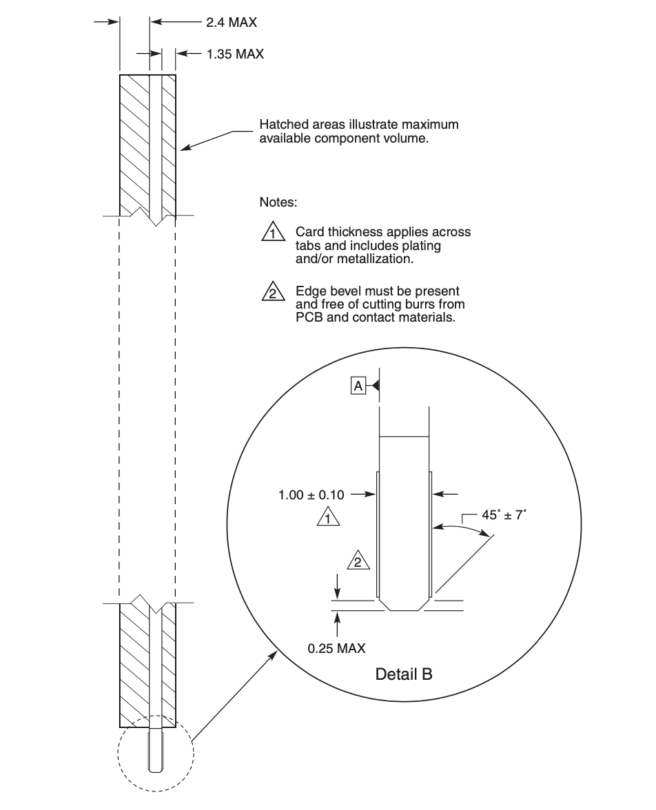
[12-AUG-25] We create an mPCIe template for KiCad and adjust its gold finger and corners in places by up to 100 μm in order to bring the dimensions and hole locations into exact agreement with the drawings. The finished template is mPCIe.zip. We begin the A305301A printed circuit board layout starting with the template.
[14-AUG-25] We concern ourselves with the distribution of our 50-MHz clock to three different logic inputs. It looks like we can do this with one trace of 11 mm and another of 24 mm. On the our ALT base board, we see reflections from an unterminated 1-m transmission line that are just enough to cause clock locking failure at 8 MHz. When we terminate with 47 Ω, the reflections vanish. The speed of propagation along the 7-mil track is about 200 m/μs, making the 8-MHz wavelength 25 m. The third harmonic of 8 MHz has wavelength 8 m, and one quarter of that is 2 m. We have problems when the line is one eighth of the wavelength of the third harmonic. In the case of 50-MHz, one eighth of the wavelength of the third harmonic will be 17 cm. Our 2.4-cm tracks are seven times smaller. We will route them and see what happens.
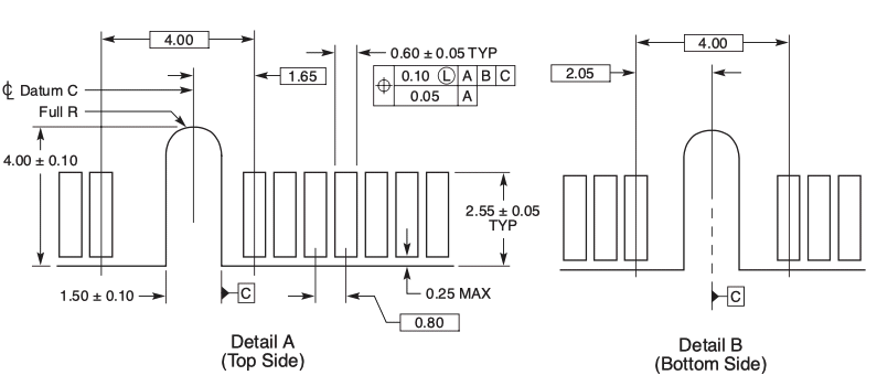
We find that our existing mPCIe template has the contact pads 0.5 mm from the board edge, when the maximum should be 0.25 mm. The contact pads are 2.0 mm long when they should be 2.3 mm long. The beveled edges on the connector end of the board should cut right to the edge of the pads, so that the pads extend to the edge of bevel.
[18-AUG-25] First draft of A305301A layout complete and checked once. All components are on the top side. Identification is on the bottom silkscreen.
[21-AUG-25] We clear the solder mask on top and bottom side of the card edge connector. We submit for fabrication. We forget to update the version timestamp on the back side of the board, so it remains 20-AUG-25, despite changes to solder masks today.
[10-SEP-25] We have our A305301A boards.
[24-SEP-25] We assemble our first A3035AV1. We load into an mPCIe socket with 3.3-V power. Current consumption with oscillator running, no program in the PIC is 51 mA.
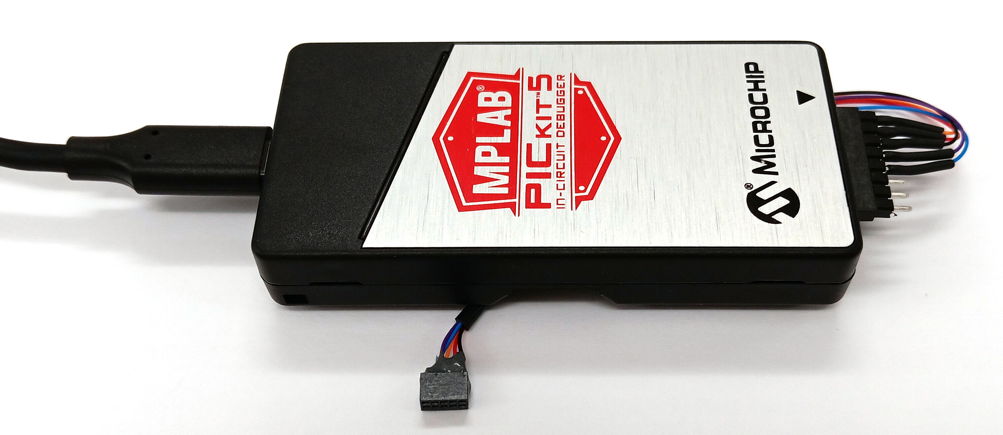
[06-NOV-25] We are programming our A3053 with our PICKit5 and adaptor cable, see PICKit5_RCM6700.jpg for a picture. Programming is reliable and fast. In P3053 we type "make" to build the "hex" file we select in the MPLAB IPE application. Our P3053 repository has undergone dramatic changes to its build structure since we copied it from the Harmony3 repository. The seven makefiles of the original repository are now consolidated into one top-level makefile. The three thousand lines of makefile build instructions are consolidated into one hundred lines. The makefile builds all C and assembler files in our src directory automatically and links them to the PIC32MZ-EF_DFP device package in our adjacent Harmony3 repository. Note that this package does not reside in the P3053 respository, but is available for download as PIC32MZ-EF_DFP.zip:.
Our TCP/IP stack is not yet working. The LAN8720A PHY is providing a link light, but we have no activity light. We have four test point LEDs connected to the RF3, RF2, RF8, and RA2 pins. These are green, blue, white, and red respectively. With our main program, we can flash the RF2, RF8, and RA2 LEDs, but the RF3 green lamp does not flash. The RF3 pin remains high-imdedance despite our efforts to set it as an output. If we short the RF2 pin to the RF3 pin, the blue and green lamps both shine brightly. The blue light does not dim when the green light shares the output.
Our programming interface is the simple, robust, two-wire interface consisting of signals PGD and PGC. It also carries 0V, 3V3, and !MCLR. It turns out that there is no way to obtain debugging information from this two-wire interface, nor will it support a console to receive messages. We direct the MUC's internal UART2 to RF8 and RF2 with the following code in our GPIO setup routine. We are writing to peripheral pin select (PPS) registers to direct RF8 to the UART2 RX input and to direct the UART2 TX output to RF2.
// Select RF8 as the source of UART2 RX. On the A3053A, RF8 is U1-58,
// connected to R11, which in turn feeds D4, the white test point LED.
U2RXR = 0b1011;

// Select UART2 TX as the source of RF2. On the A3053A, RF2 is U1-57,
// connected to, R10, which in turn feeds D3, the blue test point LED.
RPF2R = 0b0010;

// So far, on our A3053A, we have have D3 and D4 dedicated to UART2, but D2
// and D5 are available as test points. Pin U1-56 is RF3, so we want to set
// bit 3 of port F as an output. Pin U1-59 is RA2, so we want to set bit 2
// of port A as an output as well. The constants that hold the numerical
// port codes are defined in plib_gpio.h. To specify the bit, we provide a
// mask.
GPIO_PortOutputEnable(GPIO_PORT_F,0x00000008);
GPIO_PortOutputEnable(GPIO_PORT_A,0x00000004);
We configure the UART2 for 115,200 baud. We write a routine to transmit the four bytes of 32-bit integer one after another through the UART and we look at TX on our oscilloscope. The natural byte ordering on the MCU is little-endian, and the UART byte ordering is least significant bit first, so we see the 32 bits from bit0 to bit31 with a single start 0 and a single stop 1 on either end of each set of eight bits. In this way, we are able to examine the values of the GPIO control registers to see if we have configured the one for RF3 correctly. Here is the byte-transmit function and the integer-transmit function.
static void uart2_putc(char c)
{
    while (UART2_Write((uint8_t*)&c, 1) == 0);
}

static void uart2_send_int(uint32_t value)
{
	int i;
	for (i = 0; i <= 3; i++) uart2_putc(((uint8_t*)&value)[i]);
}
We test our transmit routine with 0xFFFFFFFF, 0x00000000, 0xAAAAAAAA, 0x55555555, and 0x80800101 and conclude that it is working correctly. In our main loop, we use uart2_send_int to transmit the value of the internal thirty-two bit register TRISF. Consulting table 12-13 in the PIC32MZ datasheet, this register has nine active bits corresponding to nine available pins on the chip, all from Port F.
TRISF13 TRISF12 TRISF8 TRISF5 TRISF4 TRISF3 TRISF2 TRISF1 TRISF0
The register resets to value 0x313F, for which all the above-listed bits are set (1). When one of these bits is set, the pin acts as an input. When it is clearred, the pin acts as an input. The reset value makes all the existing pins inputs. After we configure the chip, in our main loop we examine TRISF and see bits 0-15 are: 1110 1100 1000 1100. So RF0, RF1, RF2, RF4, RF5, RF12, and RF13 are inputs.

We selected RF2 as our UART2 TX output, and it is generating TX and driving the blue lamp, but TRISF2 says RF2 is an input. We configured RF3 as an output so it could drive our green LED, and TRISF2 says it is an output, but we observe RF3 to be high-impedance. We selected RF8 as the input for UART RX, we observe it to be high-impedance, and TRISF8 says it is an input. It turns out that PPS overrides TRISF, so we can now understand why RF2 acts as an output even through TRISF2 says its an input. But we still do not understand why RF3 is not driving its lamp.
[08-NOV-25] We solder three wires to our A3053A and terminate them with pins so we can more easily examine our UART2 TX, and in anticipation of connecting to a UART-USB adaptor. We use TX to look at the LATF and PORTF registers. We see PORTF3 is always LO, unless we short RF3 to RF2, in which case PORTF3 goes HI. We see LATF3 toggling as we try to toggle RF3 with our software. We replace the PIC32MZ, thinking the output transistor might be damaged. After replacement, we see exactly the same symptoms.

In the PIC32MZ datasheet, Table 3 give RF3 as pin 56 with function "RPF3/USBID/RF3". In Table 1-14 we see in the description of pin 52 "VUSB3V3" that, "USB internal transceiver supply. If the USB module is not used, this pin must be connected to VSS. When connected to VSS, the shared pin functions on USBID will not be available." We are not using the USB transceiver. We have VUSB3V3 conneced to VDD = 3V3. As a result, the USB interface is powered up, and we expect to be able to use RF3 on U1-56, but we find that U1-56 acts as an input no matter what we do with the configuration registers. We connect U1-56 to U1-50, this new pin is "OSC2/CLKO/RC15". We configure RC15 as an output and toggle it. The green LED flashes. (See 04FEB26 for resolution of this problem.)
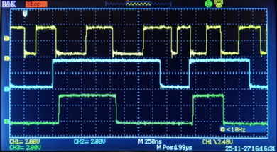
[10-NOV-25] We start work on the Ethernet PHY interface. Our link signal, LED1 is active-high, which is opposite to the !ETH signal provided by the RCM6700, so our RJ-45 socket's amber link light turns on when there is no link. It is on now. We power a full-size TCB base board with external 5 V and look at the pulses on our TX and RX lines. We see 55-ns pulses in bursts, ever few milliseconds, perhaps forty pulses separated by 30 μs. These pulses should be 100 ns, according to the Ethernet specification. We remove the A3053A, disconnect our 5-V supply and connect PoE. Now we see the pulses from the PoE switch. They are 100 ns a few times a second. We suspect that the PHY thinks that the clock we are supplying is 25 MHz, when it is in fact 50 MHz. We suspect the PIC of interfering with the three MODE straps, and build another A3053A without the PIC, only the PHY. Eventually, we determine that our pull-down strap on the PHY's LED2 (U2-2) output should be a pull-up, or it should be left floating. On the rising edge of nRST = !RST, the state of this line is clocked into the PHY to indicate the clock frequency. We remove R6, the pull-down resistor, allowing the pin to float, and we immediately get a 100 Mbps link. Our LED2 speed indicator is active-low and asserted, meaning 100 Mbps. Our LED1 link and activity indicator is ative-high and asserted, and pulsing LO occasionally to indicate activity. The amber light on the RJ-45 blinks occasionally as LED1 goes LO.
[11-NOV-25] In anticipation of writing assembler code to manage reading to and from the parallel interface and TCP/IP buffers, we obtain the following load and save instruction table from ChatGPT.
| Mnemonic | Meaning                | Bits | Sign Extension | Notes                |
| -------- | ---------------------- | ---- | -------------- | -------------------- |
|  lb      | load byte              | 8    | sign-extend    | signed char          |
|  lbu     | load byte unsigned     | 8    | zero-extend    | unsigned char        |
|  lh      | load halfword          | 16   | sign-extend    | signed short         |
|  lhu     | load halfword unsigned | 16   | zero-extend    | unsigned short       |
|  lw      | load word              | 32   | —              | standard 32-bit load |
|  sb      | store byte             | 8    | —              | writes low 8 bits    |
|  sh      | store halfword         | 16   | —              | writes low 16 bits   |
|  sw      | store word             | 32   | —              | writes all 32 bits   |
We remove R6 from our fully-populated A3053A. We program with our latest LED flashing code. We plug into our Mini-TCB. We immediately get a 100 Mbps link. We try to ping the board at 10.0.0.37, but get no answer. We examine our code, rearranging and consolidating until we see that we failed to call our the application initialization routine that defines our TCP/IP data structure. We add this instruction. We get response from ping 10.0.0.37. We get echo from telnet to 10.0.0.37:90. We tag the firmware as v1.1.
[12-NOV-25] We use the following LWDAQ Toolmaker script to measure the round-trip send and receive speed of our echo server. With ten repetitions of sending 100 kBytes and reading them back, we get a throughput of 600 kByte/s, which suggests our upload and download speeds are of order 1.2 MByte/s. Even our inefficient echo server, which reads data from the receive buffer in thirty-two byte chunks, checks every byte for the escape character, and writes the bytes to the output buffer, and sends console reports for every write to the output buffer, can almost match our RCM6700's 1.4 MByte/s. We comment out the console reporting for buffer writes and the speed goes up to 1.6 MByte/s.
set data ""
set reps 10
for {set i 0} {$i < 100000} {incr i} {append data "0"}
set len [string length $data]
LWDAQ_print $t "Length $len bytes."
set sock [socket 10.0.0.37 90]
fconfigure $sock -blocking 1 -buffering line
set start [clock milliseconds]
for {set i 0} {$i < $reps} {incr i} {
	puts $sock $data
	read $sock $len
}
close $sock
set taken [expr [clock milliseconds] - $start]
set rate [format %.3f [expr 1.0*$len*$reps/$taken/1000]]
set amount [format %.3f [expr $len*$reps/1000000.0]]
LWDAQ_print $t "Downloaded $amount Mbytes in $taken ms, $rate Mbytes/s."
We do "make clean build" and time how long it takes with optimization levels NONE, -O1, -O2, and -O3. We get x, 193 s, 209 s, and UNAVAILABLE. The -O3 optimization is available only in the x32-gcc PRO version. We update our Makefile to accept "make debug", in which case it will define the "__DEBUG" compiler macro, so that our C-code can enable console writes for debugging, and disable them for production. We connect a USB-to-UART bridge with an FTDI chip. We connect to it on our MacOS laptop using the "screen" command. We find that our TCP/IP interface advertises itself as working, but we cannot connect or ping the EEM. We build another EEM, and we can ping and telnet to that one, No2. We replace the PIC32MZ on our No1 board, still does not ping. Replace the LAN8720A, now it works. So far as we can tell, connecting our UART-to-USB bridge damaged the PHY when we disconnected the EEM from its socket and allowed the bridge to power RX. We saw both the RX and TX lamps shining, as if the entire board were powered up. We load 1-kΩ resistors in series with our UART TX and RX. WE connect our UART-to-USB bridge. We see the following in the console that the screen command creates.
screen /dev/cu.usbserial-A5041Q2Z 115200
TCP/IP Stack: Initialization Started
TCP/IP Stack: Initialization Ended - success
    Interface PIC32INT on host A3053A          - NBNS disabled
PIC32INT IP Address: 10.0.0.37
Waiting for Client Connection on port: 90
Received a connection
Server Sending hello
help

------- Supported command groups ------
 *** tcpip: stack commands ***
---------- Built in commands ----------
 *** reset: Reset host ***
 *** q: quit command processor ***
 *** help: help ***
Here we see that we connect with telnet in another terminal and send "hello". The EEM echos "hello" in that terminal, but also reports that it is sending "hello" to the console. Now we use the console, which is connected to our keyboard, to send "help" to the EEM, and the EEM responds with a help message. We have three commands available to us through the console: reset, quit, and help. We try reset, and it works.
[14-NOV-25] We eliminate the MCLAB Harmony command interface and replace it with one of our own divising. We have eliminated the Harmony system console module as well.
[17-NOV-25] Remove multiple interface support from our TCP/IP manager. Remove checking previous IP addresses. We start building the LWDAQ server by bringing over our receive-message and buffered-read routines from C2071A15.c. We are decoding the message ID and message length, reporting, and detecting both start and end codes. We now start looking into implementing the prallel interface with the base board, only to find that we have wired the chip wrong, selecting the wrong pins for the Parallel Master Port (PMP). Right now we have the following, where CA0-CA5 are the control address bus and CD0-CD7 are the mPCIe bus.
U1-6, RC1, CA0
U1-7, RC2, CA1
U1-8, RC3, CA2
U1-9, RC4, CA3
U1-91, RE0, CA4
U1-94, RE1, CA5
U1-72, RC13, CD0
U1-73, RC14, CD1
U1-98, RE2, CD2
U1-99, RE3, CD3
U1-100, RE4, CD4
U1-3, RE5, CD5
U1-4, RE6, CD6
U1-5, RE7, CD7
U1-81, RD4, !CDS
U1-82, RD5, !CWR
The correct pins for the PMP have function names PMD0-PMD15 for the data bus, PMA0-PMA15 for address bus, PMWR for !CWR, and PMRD for !CDS. Here are the pins we should use for the data bus and strobes:
| Signal | PMP func | Port | Pin | All Pin Functions          |
| ------ | -------- | ---- | ----| -------------------------- |
| CD0    | PMD0     | RE0  | 91  | EBID0 / PMD0 / RE0         |
| CD1    | PMD1     | RE1  | 94  | EBID1 / PMD1 / RE1         |
| CD2    | PMD2     | RE2  | 98  | EBID2 / PMD2 / RE2         |
| CD3    | PMD3     | RE3  | 99  | EBID3 / RPE3 / PMD3 / RE3  |
| CD4    | PMD4     | RE4  | 100 | EBID4 / AN18 / PMD4 / RE4  |
| CD5    | PMD5     | RE5  | 3   | EBID5 / AN17 / PMD5 / RE5  |
| CD6    | PMD6     | RE6  | 4   | EBID6 / AN16 / PMD6 / RE6  |
| CD7    | PMD7     | RE7  | 5   | EBID7 / AN15 / PMD7 / RE7  |
| !WR    | PMWR     | RC3  | 8   | EBIWE / AN20 / PMWR / RC3  |
| !DS    | PMRD     | RC4  | 9   | EBIOE / AN19 / PMRD / RC4  |
None of the above pins conflict with the RMII interface to our LAN8720A PHY. But two of the sixteen address lines of the PMP are used in the PHY: PMA3 and PMA11. We can make a seven-bit address bus out of PMA4-PMA10, and add PMA12 for the eighsix-bit address bus out of
| Signal | PMP func | Port | Pin | All Pin Functions                                      |
| ------ | -------- | ---- | --- | ------------------------------------------------------ |
| CA0    | PMA4     | RG7  | 11  | EBIA4 / AN13 / C1INC / ECRS / RPG7 / SDA4 / PMA4 / RG7 |
| CA1    | PMA5     | RA5  | 2   | EBIA5 / AN34 / PMA5 / RA5                              |
| CA2    | PMA6     | RC1  | 6   | EBIA6 / AN22 / RPC1 / PMA6 / RC1                       |
| CA3    | PMA7     | RB9  | 33  | EBIA7 / AN49 / RPB9 / PMA7 / RB9                       |
| CA4    | PMA8     | RF5  | 65  | EBIA8 / RPF5 / SCL5 / PMA8 / RF5                       |
| CA5    | PMA9     | RF4  | 64  | EBIA9 / RPF4 / SDA5 / PMA9 / RF4                       |
| CA6    | PMA10    | RB8  | 32  | EBIA10 / AN48 / RPB8 / PMA10 / RB8                     |
| CA7    | PMA12    | RC2  | 7   | EBIA12 / AN21 / RPC2 / PMA12 / RC2                     |
In order to use the PMP we would have to to re-wire the connections from the MPCIE to the PIC. We will proceed with a bit-banging implementation of our parallel bus that uses the connections we have.
[19-NOV-25] We are working on the LWDAQ server interface in our main.c. The programmer reports "program memory: start address = 0x1d000000, end address = 0x1d027fff", so our code appears to occupy around 160 KByte.
[24-NOV-25] We have the LWDAQ Controller Interface working with our A3053A, despite the complex selection of GPIOs we have used for the data, address, and control lines. We run the following Toolmaker script:
set sock [LWDAQ_socket_open 10.0.0.37:90]
set values [list]
foreach addr {0 3 18 19 38 40 61 62 63} {
	lappend values "$addr [LWDAQ_byte_read $sock $addr]"
}
LWDAQ_byte_write $sock 3 45
LWDAQ_stream_delete $sock 63 128 8
LWDAQ_byte_poll $sock 0 42
LWDAQ_echo $sock "[clock seconds]: Are you there Moriarty?"
set version [LWDAQ_software_version $sock]
LWDAQ_socket_close $sock
LWDAQ_print $t "version=$version"
foreach v $values {
	lassign $v addr value
  set u [expr $value & 0xFF]
	LWDAQ_print $t "[format %3d $addr] [format %4d $u]\
		0x[format %02X $u] [format %08b $u]"
}
We get the following output:
version=32
  0   42 0x2A 00101010
  3    0 0x00 00000000
 18    2 0x02 00000010
 19    6 0x06 00000110
 38    0 0x00 00000000
 40    1 0x01 00000001
 61  008 0xFF 11111111
 62    0 0x00 00000000
 63  255 0xFF 11111111
When we press the CONFIG button, we see location 40 go to zero. As we repeat the script, we see location 62, the block available counter, going up.
[28-NOV-25] We have the LWDAQ stream read working from our mini-TCB equipped with our A3053A. We examine !CDS, !CWR, and CD0 as the stream read starts up. When stream reading from the message buffer of an ALT or TCB, we have to write to the FIFO Data Strobe location (62) and then read repeatedly from that location until its value is non-zero, which indicates Message Ready (MRDY). Only then can we read a byte out of the FIFO. What we see below is two complete cycles of this sort in which MRDY is immediately set. But the first complete cycle takes twice as long as the second.
The first complete cycle is being operated with instructions being read directly from the flash memory, which runs with three wait states. The next cycle is operating out of the instruction cache, and so proceeds without memory access delays. Our existing write and read cycles both assert data strobe with five calls to lwdaq_ds_assert. The write cycle then calls lwdaq_ds_unassert. The read cycle reads the data lines before calling lwdaq_ds_unassert. Once the loop instructions are established in the instruction cache, write data strobe lasts for 125 ns, suggesting each call to lwdaq_ds_asser takes 25 ns. The read data strobe lasts for 250 ns, suggesting that assigning data line values to a byte on the stack takes 125 ns. If we zoom in on the falling edge of !CDS when we read the first 1 on CD0, the delay between !CDS asserted and CD0 going high is about 60 ns. From this we deduce that we need three calls to lwdaq_ds_assert to be sure we get the correct read value. But in practice we find that five are always required for reliable reading of zeros.
We disable the reading from the controller message FIFO, and instead transfer zeros out of our transmit buffer, so we are seeing only the TCP socket data rate. We transfer 1 MByte for a speed test and get around 6.3 MByte/s in debug and release modes. We use the following Toolmaker script for our speed test.
set n 1000000
set sock [LWDAQ_socket_open 10.0.0.37:90]
set st [clock milliseconds]
set bytes [LWDAQ_stream_read $sock 63 $n]
set dt [expr [clock milliseconds] - $st]
LWDAQ_socket_close $sock
binary scan $bytes cu* values
LWDAQ_print $t [lrange $values 0 31]
LWDAQ_print $t "[format %.1f [expr 0.001*[string length $bytes]]] kByte"
LWDAQ_print $t "$dt ms"
LWDAQ_print $t "[format %.1f [expr $n*1.0/$dt]] kByte/s"
[02-DEC-25] Our pic.c now contains routines to write to and read from non-volatile memory (NVM). Our console gives access to a string write and string read from a particular location in what Microchip calls the "program flash". This flash memory is divided into 16-KByte "pages". We can erase single pages in one operation, setting all bytes to 0xFF. Each page is divided into 2-KByte "rows". We can write single rows in one operation, but we cannot write to fragments of a row. The CPU addresses RAM, NVM, and peripherals by means of a 32-bit virtual address space set up by the microcontroller's memory management unit (MMU). Our PIC32MZ2048EFH provides 2 MByte of NVM, and this 2 MByte appears twice in the virtual address space (see Figure 4-3). The first image is from 0x9D000000 to 0x9D0FFFFF. This image is served by a memory cache: when we read from the image, the microcontroller's direct memory access (DMA) hardware transfers either a row or a page, we are not sure which, into the cache, and the CPU reads the cache. When the CPU writes, it writes to cache. At some point, if the cache fills up, the cache controller will write a row or page from cache into the NVM and read another row or page. By this means, the average access time to NVM is greatly reduced, and the CPU can execute code stored in NVM efficiently. The second image of the 2-MByte of NVM lies in virtual address range 0xBD000000 to 0xBD0FFFFF. This image is not served by a cache. Writes to this image occur directly to NVM and reads are direct from NVM. When store our own user data to NVM, we must use the non-cached image if we want to be sure that what we write will be what we immediately read back. If we write directly to NVM and read from the cached image, we will see what is in the cache, not what is in the NVM, and the cache will be out of date. We say the cache is "stale".
The PIC32MZ2048EFH provides 512 KByte of dynamic random access memory (DRAM). This 512 MByte appears twice in the virtual address space: once with chaching from 0x80000000 to 0x8007FFFF and once without caching from 0xA0000000 to 0xA007FFFF. When we copy to NVM, we do so with the DMA hardware, using the NVM_RowWrite procedure provided by plib_nvm.c. The DMA operates upon the microcontroller's physical address space. The 2-MByte NVM and 512-KByte DRAM appear only once in physical address space and there is no cache. If we fill a buffer in DRAM with 2048 bytes we want to write to NVM with NVM_RowWrite, we must make sure that this buffer exists immediately in the DRAM itself, not in the DRAM cache, because NVM_RowWrite will copy the locations from DRAM, not from the cache. We must place our buffer in the non-cached image of the DRAM. Furthermore, we must place the buffer on a suitable boundary, at least a four-byte boundary. We play it safe and put our buffer on a 32-byte boundary. Having figured out these two caching issues, our NVM write and read routines work perfectly. We can power down the A3053A and power it up again, and our string is still there. We tag the software v1.12. The console command interface allows us to write a string to NVM and read it back again.
[03-DEC-25] For the future A3053B, we no longer propose to use the Parallel Master Port (PMP) interface, but instead to simply use two available eight-bit ports for CA0-CA7 and CD0-CD7, and two other bits for !CWR and !CDS. We make a table of all the ports defined for the PIC32MZ family, then consult the pinout of our PIC32MZ100, and mark any that exist on our TQFP-100 package, and mark any that are reserved for the RMII bus, or otherwise unavailable for general-purpose use. We find that RA0-RA7 and RE0-RE7 are free an available. We propose to use RA0-RA7 for CA0-CA7 and RE0-RE7 for data bus CD0-CD7. For !CWR and !CDS we choose RA9 and RA10 respectively. We will bit-bank these registers to implement our eight-bit parallel bus. The access rate will be three or four times faster than what we have now, and plenty fast enough for a LWDAQ Driver.
[19-DEC-25] Firmware P3053A provides Command-Line Interface (CLI) on TCP/IP Telnet and UART2 Console interfaces, full implementation of all LWDAQ messages, including LOGIN, CONFIG_READ, and CONFIG_WRITE, flash memory storage of configuration, attention to configuration switch, TCP timeout and mPCIe bus routines. The debug version, with console debug prints enabled, works perfectly with our Mini TCB. But the release version, in which most console prints are disabled, fails half the time during configuration and reset of the TCB. We get a timeout reading 64 bytes with an open LWDAQ socket. No message rejection or error notifications appear in the console, the task process, or the LWDAQ message-handler.
[20-DEC-25] We install a timer in our tcp_tick routine, this being the routine that we use to maintain the stack. Instead of calling the stack and driver task routines every time we call tcp_tick, we now call them every two milliseconds. This tcp_tick_ms we add to the EEM configuration record, with a value of 2 in the factory default configuration. Now our EEM never freezes, no matter how many times we press Reset and Configure in the Receiver Instrument. We also have separate timeout periods for the Telnet and LWDAQ protocols: 10 s for LWDAQ and 300 s for Telnet.
[22-DEC-25] Version v1.20 of our P3053 software is running in a TCB streaming live data from ten A3049Q4 transmitters, a total of 20 kSPS, and being received simultaneously by six antennas makes 120 kMPS. We can re-configure and re-boot from the Configurator Tool. Our factory default configuration is identical to that of our RCM6700 LWDAQ Relays, except that we set the default LWDAQ server timeout to 10 s instead of disabling the timeout, which is much safer. The LWDAQ protocol is not designed for long-lived interactions. Our code is stable in both debug and release modes. We have consolidated the debug and release builds into one. We configure the build with constants we enter in a new config.h file. Meanwhile, all Microchip files are in a microchip directory, and we are no longer calling them "Harmony" files. Reconfiguration of the EEM takes place only by the mechanism of modifying the flash memory configuration record, then rebooting. The Telnet and Console CLIs allow us to modify the flash record. We leave the EEM running in the TCB to see if it's stable.
[26-DEC-25] We are burning in a TCB. We have 20 kSPS being fed into thirteen of the sixteen antenna inputs, for a total of 260 kMPS. We run with EEM as LWDAQ Relay and see a readout error every couple of hours. We run with RCM6700 for two days and see zero readout errors. We add two wait states to the mPCIe bus read and write cycles and start our test again with the EEM. We equip the CLI with stream read and stream write instructions, as well as a "packed" return format in which bytes are a packed string of hexadecimal digits. With "mpcie stream-read 63 512 --packed" we get a download rate of 5 kByte/s.
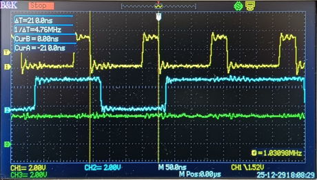
[29-DEC-25] We have implemented the LWDAQ stream write and stream read operations. We have a conditional compilation of the polling of the FIFO strobe address, so that we exclude the polling for an A2071 host. Software P3053 version v1.24 supports A2071, A3038, A3042, A3050, and A3052. We do not yet have support for A2087 hosts, which are the TCPIP-VME Interfaces. These require some further modification of byte write and read routines. Compile and test on an A2071 host, works perfectly. We test with gray-scale images and Diagnostic power supply measurements. Download speed from both these reads from RAM is 1.4 MByte/s, which is the same as for the RCM6700. We look at !CDS on the mPCIe bus driven by our A3053A and see DS pulses of 350 ns with 250 ns un-asserted in between, making 600 ns, or 1.7 MByte/s. Given that we are transmittting and flushing the socket between read bursts, in order to achive 1.4 MByte/s net download rate, the A3053A must be flushing its socket at 7±1 MByte/s. The RCM6700, on the other hand, is reading with 100-ns DS pulses and 165 ns in between, for total 265 ns, or 3.7 MByte/s. The RCM6700 must be flushing its socket at around 2.2 MByte/s.
We started with six "wait states" in our read operation. Our cycle period was 600 ns. We remove four of these wait states, leaving only two. Our cycle period drops to 520 ns. The wait state is an execution of mpcie_ds_assert(). Each execution is taking 20 ns, which is four PIC32MZ instruction cycles. With two wait states, access on the read is reliable on the A2071 host, and we have 1.6 MByte/s download. We replace our mpcie_ds_assert() wait states to deterministic NOP instructions, each of which takes 5 ns at the PIC32MZ's 200-MHz clock speed. After some experiments, our read cycle is: set up the address, make the data lines tri-state, unasserting !CWR, waith 50 ns, assert !CDS, wait 50 ns, read data bus. We switch to using the repeat-read, in which we do not have to set up the address, so our repeat-read is: assert !CDS, wait 50 ns, read data bus. We re-work the data-get routine so it puts together registers C and E to make the data bus more quickly. The cycle time for the repeat-read is 210 ns, which is 4.8 MHz. Our block download speed is now 2.6 MByte/s, suggesting TCP download at 6±0.5 MByte/s.
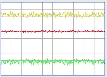
We are obtaining nice BCAM images. We compare noise for blank images and find it to be 0.5 cnt rms for the A3053A-equipped driver and only 0.4 cnt rms for the RCM6700-equipped driver. The driver passes all Driver Checker tests except one: The Diagnostic Instrument power supply measurements are noisy and inaccurate. The 15-V supplies have average values +16.4 V and −15.6 V. This is nothing to do with fast readout: we add 100-ns delays to the readout cycles and nothing changes.
We return to our Telemetry Control Box (A3042). With no added delays, we see immediate failure trying to identify the TCB. We add a compiler flag to control addition of further delays for the TCB and ALT: MPCIE_SLOW_ACCESS. With this flag defined, we add 50 ns delay before end of DS on write and before data latch on read. Our No2 A3053A is able to support recording in a TCB for one minute without errors. Our No1 A3053A will identify itself, but we see read errors within seconds. We increase the slow-access delay from 50 ns to 100 ns. The No1 and No2 boards are both now stable over minutes.
[30-DEC-25] We try our A3053A in a TCB during stress testing with 320 kMPS (20 kSPS on each of 16 antenna inputs). We see occasional data corruption errors in the Neurorecorder. We disconnect 2 of the 16 antennas, dropping the message rate to 280 kMPS and we see no errors in several hours. But we do see "extra samples" warnings in the Neuroplayer. We compare to the RCM6700, for which we see no no data corruption errors at 320 kMPS, but we do see "extra samples" warnings. We conclude that the A3053A as it is today is slower at reading, which has a slight effect upon the maximum message rate.
We open the Stimulator Tool from the Neuroplayer and use it to command some stimulators, while at the same time recording 280 kMPS with the TCB using an independent Neurorecorder. We now have two clients wanting access to the TCB. With the RCM6700, the sharing of the TCB is graceful: socket connections are queued. Each client need wait only a few seconds before being serviced. But the A3053A has not socket queue. When a client tries to connect, if the A3053A is busy, it ignores the connection request. The request times out and the client tries again. The result is a chaotic arbitration between competing clients leading occasionally to a timeout and an error.
[12-JAN-25] Firmware v1.29 provides a four-spot queue for each server. We can now queue up to four LWDAQ connections and four Telnet connections. Each server serves only one socket at a time, as did our RCM6700. We have consolidated the mPCIe access wait states into the ds-assert routine, where we have a setup and a hold delay before and after assertion of data strobe respectively. For the A2071E we are using 50 ns for setup and 100 ns for hold. On the A3042 we are using 100 ns and 200 ns respectively. We are running for hours with no errors. Download speed for a block of image data from the A2071E is now 1.7 MByte/s rather than 2.6 MByt/s because we are inserting the hold delay in the stream reads, which is unecessary. Our issue with the A3053A introducing noise into the LWDAQ Driver power supply monitor has resolved itself. We now get clean power supply measurements after re-arranging the wait states in the mPCIe access routines and fixing a bug in the mPCIe write routine. We can only assume that the error was not a real issue with the power supplies, but corruption of our measurements by read errors.
[13-JAN-26] Firmware v1.30 redistributes the setup and hold delays in the mPCIe access routines. We now have a settling delay in the set-address routine, which is 50 ns or 100 ns for normal and slow access. We have an access delay after asserting data strobe, which is 100 ns or 200 ns for normal and slow access. With fast access on an A2071E, the stream read period is 260 ns (3.8 MByte/s) and the stream downoad rate is 2.1 MByte/s (so TCP/IP dowload is 4.7 MByte/s). The stream read no longer includes the settling time for address, so it runs fatster than v1.29. In our access routines, we use the address settling time to settle the control write line and the data bus as well, so these changes to the bus must precede setting the address. We drop the access delay from 100 ns to 50 ns for normal speed readout. Stream read period is now 210 ns. We see reliable reads and writes from RAM and download of about 2.3 MByte/s. But we also see power supply noise of about 2 Vpp. We revert to the 100 ns access delay. Over local wired network we once again see 2.1 MByte/s. Over our wireless network we see 1.7 MByte/s. Fix some problems with LWDAQ configuration messaging, firmware v1.31. We now have one A3053A running in a TCB and another running in an A2071E, both in constant or regular use. We run three separate LWDAQ programs and download TC255P images from the same S0199 driver simultaneously, thus exercise the server queue, which contains four slots. We get no data acquisition errors. Each BCAM is downloading 1.7 images/s for a total of 6.7 images/s. We set up five Dosimeters downloading simultaneously and see no errors. It appears that the active and listening sockets, in addition to the four-slot queue, can handle five clients. But when we increase to six Dosimeters, we start to see errors.
[14-JAN-26] In firmware v1.34, we can redirect console messages to any other CLI channel. In particular, we can redirect to a Telnet channel with "debug grab", and restore to the UART2 console with "debug release". We compare Diagnostic Instrument voltage measurement download speed with debug off, debug on and UART2, and debug on and Telnet. We get 2.2 MByte/s, 1.7 MByte/s, and 2.2 MByte/s. Sending debug message to the Telnet interface does not appear to slow us down at all.
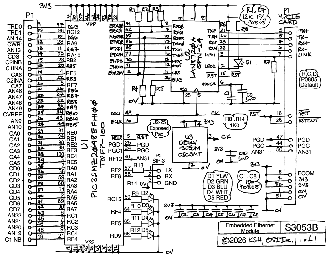
We prepare S3053B, schematic for the A3053B with changes listed in the modifications chapter. We have control data all provided by RA0-RA7 in order, control address by RE0-RE7 in order, !CDS on RA10 and !CWR on RA9.
#ifdef EEM_MODULE_A3053B
#define MPCIE_CAB_MASK      0x000000FFu  // RE0-RE7
#define MPCIE_CDB_MASK      0x000000FFu  // RA0-RA7
#define MPCIE_CDS_MASK      0x00000400u  // !CDS=RA10
#define MPCIE_CWR_MASK      0x00000200u  // !CWR=RA9
#endif
When we are performing quality control on a batch of SCTs with the A3053A in our LWDAQ Driver, we get corrupted data errors once every thirty seconds. These we previously associated with readout with insufficient access time. We increase the access time for normal access from 100 ns to 150 ns, leaving the slow access at 200 ns. Now we see no read errors from our LWDAQ Driver.
[04-FEB-26] We discover that setting FUSBIDIO to "OFF" in initialization.c turns off the USB interface and allows U1-56 to be used as RF3. We remove the little wire we had joining U1-50/RC15 to U1-56, and instead use U1-56 directly as originally planned. We finally have U1-56 as an output. We change both the S3053A and S3053B schematics to restore D2 to being driven by U1-56.
#pragma config FUSBIDIO = OFF
[06-FEB-26] We submit the A305301B for fabrication. We failed to reverse the polarity of the PHY's Ethernet activity output, so we expect the light on our RJ-45 socket to turn on when there is no link.
[03-MAR-26] We are starting our CrowdSupply campaign to see if there is sufficient interest in the EEM to justify a run of 250 circuits. We are estimating the cost with an idea of estimating the correct price in quantity 250. Crowd supply will take 15.75% of the gross revenue (12% share of proceeds, 3.75% credit card processing). They charge a $5 per-item fee. The cost of components in quantity 250 at Digi-Key is $16.21 per board. To estimate the cost of assembly, we start with the 2023 assembly price of our mPCIe A3038DM-D3 boards, which were double-sided with 76 components. These were $5434 in quantity 200. Our A3053BV1 EEM has 34 parts and is single-sided. Allow 10% increase for three years inflation and we have $13.37 per board in quantity 200, let's use this for our assembly cost. Our costs are $34.58 plus 15.75% of price. If we want our price to be twice our costs, we have to charge around $100 per assembly. That way, we pay CrowdSupply $20.75, we pay Digi-Key $16.21, we pay the assembly house $13.37, and we keep $50 for ourselves.
[06-MAR-26] We have in hand our A305301B printed circuit boards. We start assembling two of them.
[08-MAR-26] Telnet interfaces working on our first two A3053B. Working on the mPCIe pin assignments. We record below the final pin assignments of the A3053A. We are about to replace these in them M3053 manual page.
| A3053A Signal | mPCIe Contact | A3053A Signal | mPCIe Contact | A3053A Signal | mPCIe Contact |
|---|---|---|---|---|---|
| 0V | P1-1 | U1-22, RB3 | P1-19 | U1-72, SOSCI/RC13 | P1-35 |
| +3V3 | P1-2 | U1-23, RB2 | P1-20 | U1-73, SOSCO/RC14 | P1-36 |
| U2-21, TXP | P1-3 | U1-26, RB6 | P1-21 | U1-98, RE2 | P1-37 |
| U2-23, RXP | P1-4 | U1-27, RB7 | P1-22 | U1-99, RE3 | P1-38 |
| U2-20, TXN | P1-5 | U1-32, RB8 | P1-23 | U1-100, RE4 | P1-39 |
| U2-22, RXN | P1-6 | U1-33, RB9 | P1-24 | U1-3, RE5 | P1-40 |
| U2-3, LINK | P1-7 | U1-34, RB10 | P1-25 | U1-4, RE6 | P1-41 |
| ECOM | P1-8 | U1-43, RB14 | P1-26 | U1-5, RE7 | P1-42 |
| U1-97, RG13 | P1-9 | U1-44, RB15 | P1-27 | U1-28, RA9 | P1-43 |
| U1-2, RA5 | P1-10 | U1-15, !MCLR | P1-28 | U1-24, PGEC1/RB1 | P1-44 |
| U1-10, RG6 | P1-11 | U1-6, RC1 | P1-29 | U1-19, RE9 | P1-45 |
| U1-82, RD5 | P1-12 | U1-7, RC2 | P1-30 | U1-38, TCK/RA1 | P1-46 |
| U1-11, RG7 | P1-13 | U1-8, RC3 | P1-31 | U1-25, PGED1/RB0 | P1-47 |
| U1-81, RD4 | P1-14 | U1-9, RC4 | P1-32 | U1-17, TMS/RA0 | P1-48 |
| U1-18, RE8 | P1-15 | U1-91, RE0 | P1-33 | U1-39, TDI/RF13 | P1-49 |
| U1-15, !MCLR | P1-16 | U1-94, RE1 | P1-34 | U1-40, TDO/RF12 | P1-50 |
| U1-20, RB5 | P1-17 | 0V | P1-51 | ||
| U1-21, RB4 | P1-18 | +3V3 | P1-52 |
[09-MAR-26] We have P3053 v2.2 running perfectly with the A3053B on a TCB. We have P3053 v2.3 running perfectly on a LWDAQ Driver. When we compare the A3053A and A3053B download speed with the Diagnostic Instrument form our A2071E, we get the same 2.3 MByte/s average rate for both. We add a "lamp" command to the CLI so we can turn on and off lamps D2-D5, which are available on the A3053B. We add to our TCPIP server structure two function pointers for routines that turn on and off a socket active indicator. We use these to turn on the blue lamp for Telnet and the white lamp for LWDAQ sockets.
[19-MAR-26] We have an A3053B loaded in our A2071 LWDAQ Driver with IP address 192.168.1.11. This device is connected to our wired network through a PoE switch, but obtains its power from a 24-V adaptor. Once a day we fail to contact this server and have to reset the entire driver. We open the box and leave it open. This morning the red lamp on the A3053B is blinking off. The driver's front-panel LINK light is flickering off. The RJ-45 socket activity lamp is flickering off. We connect a UART-to-USB bridge. The console says "DRV_PHY operation error: -5". The CLI status command reports that the link is DOWN and the network is UP. The IP address and gateway are correct.
The A3053B connects !RSTIN to !RSTOUT on the mPCIe, !MCLR on the PIC32MZ, and !RST on the LAN8720A. The PIC32MZ cannot drive its own !MCLR. It can reset itself, but it cannot reset the LAN8720A. Nor does the host board logic on our A2071E provide any way to drive !RSTIN LO through software. If we detect a failure of the PHY after a few hours, the only certain way to get it to reboot is to drive !RST LO. We resolve to separate !RSTIN from !RSTOUT in the A3053C. We add a pull-up to !RSTOUT and connect it to both the mPCIe P1-28 and to the LAN8720A's !RST input. Now we can drive !RSTOUT LO using an open-drain output on the PIC32MZ. The host board can reset the PIC32MZ with !RSTIN, and the PIC32MZ will subsequently reset the LAN8720A. The host board can make use of !RSTOUT as well, if it likes. The PIC32MZ will never drive !RSTOUT HI.Now that we are resigned to generating a new layout A305301C, we add three more test point pads to the board and connect them to RC15 (U1-50), RD1 (U1-76), and RD4 (U1-8 1). We mark all three on the top overlay with their PIC32MZ names.
[23-MAR-26] The A3053B loaded in our A2071 LWDAQ Driver went three days without its PHY having any problems. We connect to it this morning. Soon after, however, when we are moving things around on our workbench, the PHY disconnects. We reset with front panel button and all is well, but the same failure occurs two more times in the next few hours. Meanwhile, an A3053B in a Mini TCB on our workbench is idle and always connected, while an A3053B in our A3042B-16 operates continuously without interruption.
| mPCIe Pin |
A3053C Signal |
RCM6700 Signal |
mPCIe Pin |
A3053C Signal |
RCM6700 Signal |
|---|---|---|---|---|---|
| 1 | P1-1, 0V | GND | 27 | P1-27, U1-44, RB15 | PB0 |
| 2 | P1-2, +3V3 | +3.3 V | 28 | P1-28, U1-1, !RST | !RESET_OUT |
| 3 | P1-3, U2-21, TXP | Tx+ | 29 | P1-29, U1-91, RE0 | IA0 |
| 4 | P1-4, U2-23, RXP | Rx+ | 30 | P1-30, U1-94, RE1 | IA1 |
| 5 | P1-5, U2-20, TXN | Tx− | 31 | P1-31, U1-98, RE2 | IA2 |
| 6 | P1-6, U2-22, RXN | Rx− | 32 | P1-32, U1-99, RE3 | IA3 |
| 7 | P1-7, U2-3, LINK | LNK | 33 | P1-33, U1-100, RE4 | IA4 |
| 8 | P1-8, ECOM | ECOM | 34 | P1-34, U1-3, RE5 | IA5 |
| 9 | P1-9, U1-97, RG13 | PE0 | 35 | P1-35, U1-17, RA0 | PA0 |
| 10 | P1-10, U1-96, RG12 | PE1 | 36 | P1-36, U1-38, RA1 | PA1 |
| 11 | P1-11, U1-10, RG6 | PE2 | 37 | P1-37, U1-59, RA2 | PA2 |
| 12 | P1-12, U1-28, RA9 | PE3 | 38 | P1-38, U1-60, RA3 | PA3 |
| 13 | P1-13, U1-11, RG7 | PE5 | 39 | P1-39, U1-61, RA4 | PA4 |
| 14 | P1-14, U1-29, RA10 | PE6 | 40 | P1-40, U1-2, RA5 | PA5 |
| 15 | P1-15, U1-23, RB2 | PE7 | 41 | P1-41, U1-89, RA6 | PA6 |
| 16 | P1-16, U1-15, !MCLR | !RESET_IN | 42 | P1-42, U1-90, RA7 | PA7 |
| 17 | P1-17, U1-20, RB5 | PD0 | 43 | P1-43, U1-6, RC1 | !IORD |
| 18 | P1-18, U1-4, RE6 | IA6 | 44 | P1-44, U1-24, PGD | VBAT_EXT |
| 19 | P1-19, U1-22, RB3 | PD2 | 45 | P1-45, U1-7, RC2 | !IOWR |
| 20 | P1-20, U1-5, RE7 | IA7 | 46 | P1-46, U1-8, RC3 | SCLKA/IA7 |
| 21 | P1-21, U1-26, RB6 | PC0 | 47 | P1-47, U1-25, PGD | STATUS |
| 22 | P1-22, U1-27, RB7 | PC1 | 48 | P1-48, U1-9, RC4 | TXA/PC6 |
| 23 | P1-23, U1-32, RB8 | PC2 | 49 | P1-49, U1-21, RB4 | SMODE |
| 24 | P1-24, U1-33, RB9 | PC3 | 50 | P1-50, U1-40, RF12 | RXA/PC7 |
| 25 | P1-25, U1-34, RB10 | PC4 | 51 | P1-51, 0V | GND |
| 26 | P1-26, U1-43, RB14 | PC5 | 52 | P1-52, +3V3 | +3.3 V |
[25-MAR-26] The mean time between failures of our A2071E's A3053B is decreasing. Today it failed repeatedly. We exchange for a different A3053B, which we program for the A2071E. We put the first A3053B in a mini TCB and program for A3042. The one that failed in the A2071E is now stable in the mini TCB. The new one in the A2071E is failing repeatedly. We swap the A2071E's short blue shielded Ethernet cable for a short white unshielded cable. The A3053B in our A2071E is stable with this new cable. We throw the old cable away.
[26-MAR-26] Our A2071E's A3053B is still running well with the new cable. Two others in TCB base boards continue to run for days without any problems.
[27-MAR-26] We pulled the power chord out of our work bench power strip at some point this morning, then plugged it back in again. The A2071E's A3053B will not complete booting up, not matter what we do. We unplug power and plug in again. We press reset. We unplug network cable and plug in again. We remove from mPCIe socket and plug in again. We try doing multiple things at the same time, and we always get:
===========================================================
=========    Embedded Ethernet Module Console     =========
===========================================================
The debug flag is not set, expect quiet output.
TCP/IP Stack: Initialization Started
DRV_PHY operation error: -1
DRV PHY init failed: -1
TCP/IP Stack: Interface Initialization failed: 0x0 - Aborting!
We remove the A3053B. We scrub the mPCIe socket with a brush. We clear it with hand blower. We scrub the mPCIe board edge contacts. We plug the card in again. It starts up perfectly. We cycle power, unplug A3053B and plug in again, starts up every time. Put lid on box, restore A2071E to its place on bench, ten minutes later, it's not responding. Restart, it responds.
[30-MAR-26] Our A2071E with A3053B is still online. Our hypothesis right now is that the mPCIe contacts on the A2071E host board were dirty. Complete schematic of the Demonstration Board. The board provides testing for fast bus access by means of an eight-bit counter that increments at the end of every bus cycle, provided CA7 = 0. Otherwise it does not increment.
[10-MAY-26] Three A3053B working every day, no need to reboot. We submit A305301C for fabrication. The new board separates the PIC reset from the PHY reset. We have !MCLR entering the board as before, but passing only to the !MCLR input on the PIC. We have another GPIO assigned to act as !RST, which will be open-drain, and this one resets the PHY and leaves the board on !RST_OUT.
[30-JUN-26] We measure 5.0 V current consumption of the A3038BB-D4 TCB Base Board. With RCM6700 loaded, we see 1.46 A flowing in through 5.0 V. We remove RCM6700 and see 1.19 A. We load A3053B EEM and see 1.35 A. It looks like the A3053B is responsible for 750 mW. But we are converting 5.0 V to 3.3 V with an 80% efficient converter, so the power dissipated by the A3053B is closer to 600 mW, with current 180 mA at 3.3 V. The RCM6700, meanwhile, consumes 1.0 W.
[01-JUL-26] We have our first assembled A3053C on the A305301C PCB with hard gold fingers. Both work perfectly. On software reaset, the PIC now asserts its local !RST, which resets the Ethernet interface. This means we can reset the Ethernet interface with either the LWDAQ or CLI instructions. We abandon our Crowd Supply campaign. We have nine subscribers after three months, out of a target of 150 for launch.