| Brandeis University | Physics 29a |
| Spring 2020 | Kevan Hashemi |
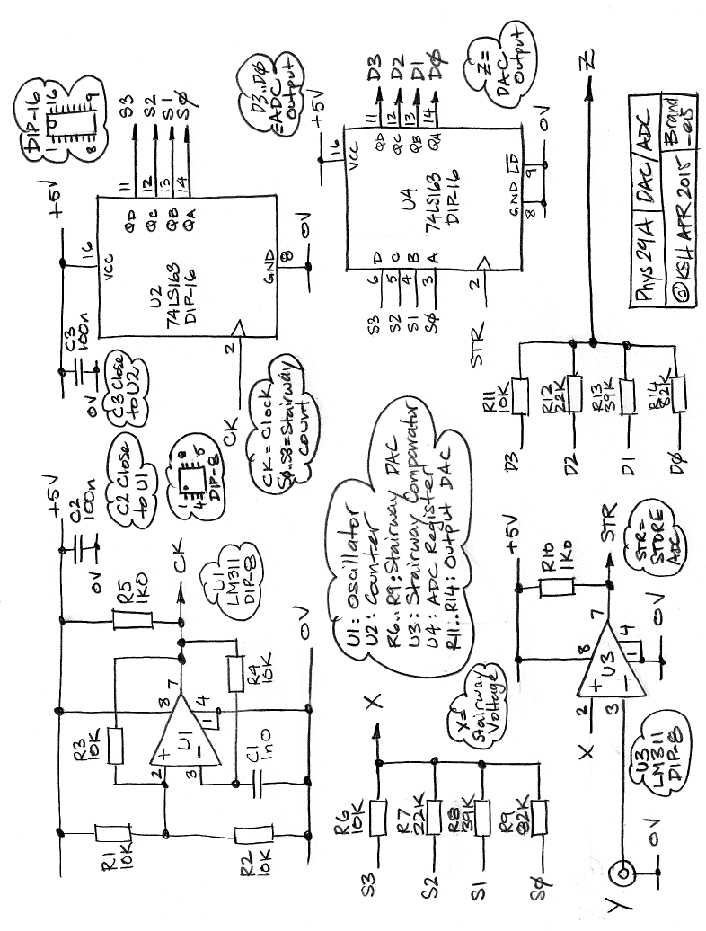
Note: For Part 1, draw your own circuit diagram. For Parts 2 onwards, work from the circuit diagram on the next page.
Part 1: Design and build a memory cell using combinatorial logic gates. Input A appears on output B when we assert input WRITE, but otherwise B retains its current value. Draw a circuit diagram of your memory cell, including pin numbers and power supply connectionss. Demonstrate your memory cell to an instructor.
Part 2: Design and build an edge-triggered latch using combinatorial logic gates. Input A appears on output B when we apply a rising edge to input CK, but otherwise B retains its current value. Draw a circuit diagram of your latch. Demonstrate your latch to an instructor.
Part 3: Consulting the circuit diagram on the next page, build the clock oscillator, which consists of comparator U1 and surrounding resistors and capactiors. Measure the frequency of the clock signal, CK, for C1 = 1.0 nF, 10 nF, and 100 nF. How does the clock frequency vary with capacitance? By decreasing C1, what is the highest clock frequency you can attain? At this highest frequency, will the oscillator still run without the decoupling capacitor, C2?
Part 4: Restore C1 to 1.0 nF and check the oscillator is running well. Build the stairway counter, which consists of U2 and C3. Draw a timing diagram showing how the four stairway bits, S0..S3, evolve over sixteen complete cycles of CK. How would this timing diagram change if you inserted an inverter between CK and the clock input of U2?
Part 5: Build the stairway digital to analog converter (DAC), which consists of R6..R9. Sketch the stairway voltage, X. How many steps do you see? What is the smallest step size, and the largest? Give two reasons why the step sizes are not uniform.
Part 6: Build the stairway comparator, which consists of U3 and R10. Drive the analog input, Y, with a potentiometer so we can vary it from 0 to 5 V. Look at STR on your oscilloscope while increasing Y from 0 to 5 V. Does the frequency of STR change? Does its duty cycle change? What event causes the falling edge of STR? What event causes the rising edge of STR?
Part 7: Build the analog to digital converter (ADC) register, which consists of U4. Which is the most significant bit of the register? How does the binary number D3..D0 vary with Y?
Part 8: Build the output DAC, which consists of R11..R14. Observe how Z varies with Y. Connect a triangle wave of 100 Hz to Y. Compare Y and Z on your oscilloscope. What are the minimum and maximum values Z can attain? Adjust the amplitude and offest of Y until the triangle wave lies just within the range of Z. Sketch the two waveforms.
Part 9: What is the average sampling frequency of your ADC? What is the ratio of clock frequency to sampling frequency? Switch to a sinusoidal waveform on Y. What is the highest frequency of sinusoid that still appears as a waveform of the same frequency on Z? Set your clock frequency to the maximum value you obtained in Part 3. What is the maximum frequency sinusoid you can apply to Y and see a waveform of the same frequency on Z?