 A3042B-4
[04-AUG-26] This page is the record of the testing and troubleshooting performed for the A304205A 4-way telemetry control box printed circuit board. The initial tests and their respective goals will be outlined here in the introduction, and will be elaborated on in their respective sections below.
It must be established that the Power Over Ethernet (PoE) circuit works. This will be determined by measuring the voltage of VCC - VEE and VCI+ - VEE as the board is plugged into PoE. VCI+ - VEE should rise to something of the order of 50V, and VCC - VEE should do the same. It must be determined that these are adequately powering the 5V DCDC converter, and this will be determined by checking whether it is producing 5V when PoE is connected.
The board first has the RJ45 PoE socket loaded. 6/6 BNC-RA connectors, 4/4 push buttons, and 1/5 MPCIE socket's are also loaded to determine how well the board fits in it's aluminum chassis.
First, the parts that connect VCI+ and VCI- to the VEE and VCC power supplies must be loaded. The following are loaded onto the A304205A printed circuit board:
R1, R2, R3, R5, R6 (25k)
(Note that since 25k 0805 resistors are out of stock, two 49.9k resistors in parallel will be substituted.)
R4 (1M0)
C1 (1n0 50V)
Q1 (DMN67D7L)
Q2 (ZXTP2025F)
Z1 (BZX84B33-FP)
Once these are loaded, VCI+ and VCI- are connected to circuit power (VEE and VCC). It should be noted that VEE and VCI- are the same 'net', which is to say they are really two names for the same voltage. From now on, only 'VEE' will be used to refer to this voltage, because this is what it is labeled as on the PCB silkscreen, and also to minimize confusing repetitions and excessive arithmetic symbols.
R1 of this circuit is intended to provide the 25k Ohm 'signature' to the Power Sourcing Equipment (PSE). The PSE is what delivers the power through the ethernet cable, and is responsible for checking for this signature before it sends full power to the powered device. In this case, a 4-way "TP Link" PoE switch is the PSE.
Since 25k resistors are out of stock, 49.9k resistors in parallel are substituted wherever 25k is called for.
The PSE should send out a 2-10V pulse to check for the 25k signature. If the signature is detected, 56V will be sent through the PoE. If less than 10 mA is drawn from the board for over 250 ms of power being supplied to the board, the PSE will shut off power. Therefore, a load has to be attached to the board power (VCC - VEE) to draw at least 10 mA to allow for power to be continuously supplied. To achieve this, the 5V DCDC converter (SPB06G-05) will be loaded along with it's associated decoupling capacitor and inductor.
The following are now loaded onto the board:

L1 (SPBW06G-05)
L2 (10 uH p1210)
C5 (1u0) (Note that schematic calls for 250V, however 50V is all that's available)
An oscilloscope will measure the following voltages:
(VCI+ - VEE): 0-56V power over ethernet
(VCC-VEE): Board power voltage, supplying L1
(5V - 0V) : The 5-volt output from L1
The oscilloscope probes are arranged in the following:
Ch1 (Yellow): A 2-alligator-clip BNC cable is attached to CH1 on the scope. Red clip is hooked to VCC, and black clip is hooked to VEE.
Ch2 (Blue): A 2-alligator-clip BNC cable is attached to CH2 on the scope. Red clip is hooked to VCI+, and black clip is hooked to VEE.
Ch3 (Green): A pin-and-clip BNC cable is attached to CH3 on the scope. Pin is inserted into 5V test point, and clip is hooked to 0V pad on board edge.
To run PoE to the board, an ethernet cable connects port 1 of a PoE switch to an ethernet socket. A second cable is joined to Switch-2, port 2 of the ethernet switch. The switch itself is powered by it's power supply from a wall socket.
Switch-2 is connected to the board's RJ45 socket, and the oscilloscope is triggered.
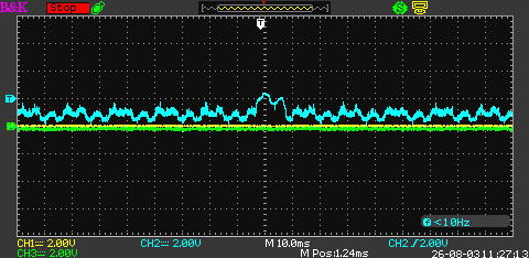
The oscilloscope shows 0V on CH1 and CH3. CH2 shows an oscillating voltage, which dips to ~0.5V and rises to a ~1V with a period of about 5 ms.
Upon closer inspection, a peak slightly over 2V appears periodically, independent of the 0.5V oscillation. This peak lasts for about 10 ms. This suspected to be the PSE probe voltage:
To determine whether this is the PSE probe pulse, and whether the 25k signature is not being presented to the PSE, R1 is replaced with 24k + 1k in series (instead of 2 x 49.9k). The board and RJ45 interior are blown extra dry, and the board is left to sit out to dry for several minutes.
Using a digital multimeter, resistance across VCI+ - VCI- is 24.76k (measured from test points). This is within 1% of the required signature.
After leaving the board to dry for several minutes, the board is hooked up again to the scope and the ethernet cable is attached. A similar result is observed, with a ~2V 10 ms peak occurring every >180 ms. The VCC-VEE voltage however is observed to decrease from 0 to ~-3V at the same time as the pulse, and remains at -3V until a second pulse, at which point it further decreases to -4.5V over the course of the 10 ms pulse, before increasing back to 0V from the end of the pulse:
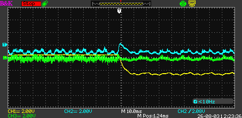
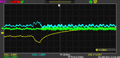
Upon further examination, this behavior of VCC-VEE is not immediately reproducible, and the oscilloscope readings return to the usual pulses in VCI+ - VCI- with consistent 0V on VEE-VCC.
Measuring the resistance across the VCI+- pins of the RJ45 connector directly (pins 9 and 10), the resistance is still 24.75k.
While checking equipment, the cable connecting the PoE switch to the ethernet wall socket was disconnected, and this caused the "power" light on port 2 of the switch to begin blinking. Note that port 2 is the port that the A3042B-4 is hooked up to.
When power is connected to the board, VCI+ - VEE jumps to 12V and remains there for about 300 ms. about a full second later, there is another square pulse lasting 300 ms, but only rising to 2V. VCC-VEE does not rise any higher during the larger 12V pulse than it does during the small 2V pulse.
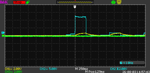
After some basic manupilation of the board (Literal handling, picking up, turning around, plugging and re-plugging PoE) the amplitude of the square wave settled to an out-of-range value.
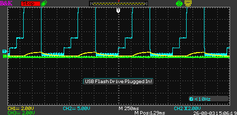
The ~300 ms duration of these pulses suggest that the PoE is shutting off due to the required 10 mA not being drawn by the circuit. The loaded parts are inspected for bad joints.
No bad joints are found. Maybe the DCDC converter is not drawing enough current. The datasheet for SPB06G-05 lists 4 mA as the no-load input current, which would not meet the 10 mA requirement. To see if this is the cause, a load must be placed at L1's 5V output. To make things as simple as possible, the load will be chosen such that it satisfies L1's 'full load' requirement. L1 can produce up to 600 mW at 5V, so a resistor of about 42R should 'fully load' it. A higher resistance would reduce the current of the output, thus the power out, and so would reduce the power consumed as well.
To test whether the DCDC current consumption is the limiting factor, we will attempt to load L1 and see whether we can increase the current consumption. To do this, 44R is loaded to the board joining the pins 5 and 6 of L1 (5V and 0V respectively).
This test produced the same result as when L1 was not loaded with any resistors.Q1's gate voltage will be measured.
The datasheet of Q1 (DMN67D7L) says that the gate threshold voltage is 1.3V - 2V. Measuring the voltage between Q1-2 (Q1 base) and VEE when, there appears to be 11V:
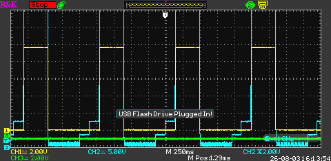
[5-AUG-2026] To examine the behavior of the circuit at lower voltages, a benchtop power supply will be used to power VCI+ - VEE instead of power over ethernet. A 30V-max power supply and oscilloscope are set up on the board, and 10V is applied to VCI+ - VEE. Voltage remains zero at VCC-VEE and 5V, and with the use of a digital multimeter is measured to be zero at Q1-base.
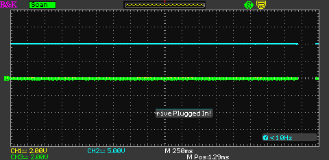
20V is now applied to VEE-VCI+. No difference is observed. 30V is applied, and again no difference is observed.
A second 30V-max benchtop power supplies is connected in series with the first, after verifying that they do not have an internal ground (Resistance between -V and GND are measured to be very high).
Power is supplied at 30V and is increased gradually to 51V. Once power supply gets over 33V, VCC-VEE voltage begins increasing slightly, never growing past 1V. When 36V is supplied, Q1-base voltage is around 1.6V. As voltage is increased to 51V, VCC-VEE never jumps up to meet VEE-VCI+.
[08-AUG-2026] It was discovered that there is an apparent discrepancy between the Q1 pinout on the A3042B-4 schematic and the Q1 package. The A3042B-4 board has been laid out according to the schematic. On the schematic, Q1-base is denoted as Q1-2, Q1-collector is denoted as Q1-1, and Q1-emitter is denoted as Q1-3. That is to say, on the schematic, Q1-2 is routed to R2-2 (R2 in series with Z1), while Q1-1 is routed to R6-2 (R6 in series with VCI+) and Q1-3 is routed to VEE. Therefore with this layout, Q1-2 will rise to 2V at a board power of about 36V, after which point Q1-1 is expected to drop to near VEE. However, the pin designated on the schematic as Q1-2 (Bottom right of package when lone pin points up) is apparently not the base but the emitter, and Q1-3 (Bottom left of package when lone pin points up) is apparently not the emitter but the base.
In light of this apparent discovery, Q1 has been replaced with a new component of the same part, that is, with another component out of the same reel as the old one. This Q1 replacement is loaded onto the board upside down, with it's belly facing up.
The pin of Q1 which is now understood to be the base will be referred to as Q1-base. Q1-base is routed to R2-2, which is in series with Z1. Therefore as the voltage VCI+ -VCI- is raised above 33V, Q1-base is expected to rise to about 2V. Q1-base was formerly Q1-2, and is now Q1-3.
The pin of Q1 which is now understood to be the emitter will be referred to as Q1-emitter. Q1-emitter is routed to VEE. Q1-emitter was formerly Q1-3, and is now Q1-2.
The pin of Q1 which is understood to be the collector will be referred to as Q1-collector. Q1-emitter remains unchanged as Q1-1.
Scope probes are attached to Q1-base, Q1-emitter, and Q1-collector. Each probe is grounded to VEE. Benchtop power supply is attached to board power (VCI+ - VEE). Board power is raised from 0V to 30V. Note that CH1, CH3, CH4 are all set to -20V, meaning as they increase from the bottom of the screen they are increasing from 0V.
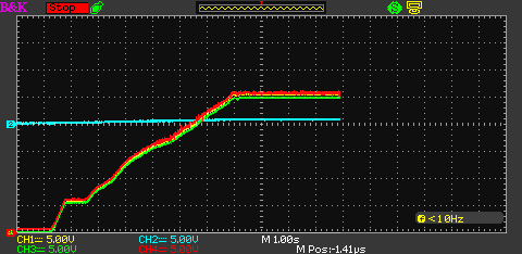
Board power is raised from 30V to 50V. Note that CH1, CH3 and CH4 are now set to -40V, meaning as they increase from the bottom of the screen they are increasing from 20V:
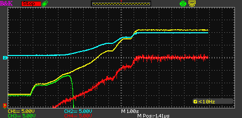
Next, the board will be connected to power-over-ethernet to determine whether 5V is being produced. The board is connected to an ethernet switch. 5V is measured on the scope. When the PoE cable is joined to the board, VCI+ - VEE and VCC-VEE jump to around 50V. 5V power is supplied to the test point. The 3V3 and transmit LED's are illuminated. it is concluded that PoE is now working.
Setting aside the PoE switch, benchtop power supplies are used to power VCC-VEE, which in turn power the first DC-DC converter that produces 5V. This DCDC converter seems to work as intended: L1 (SPBW06G-05) produces 5V at a minimum of 10V input, and continues to produce a steady 5V all the way to 56V. With a 44R load connecting the converters positive and negative outputs, a digital multimeter measures the converter current consumption to be 20 mA at 48V.
The following are loaded onto the board:
U1 (LTC3404EMS8 Buck Regulator)
R41 (1k)
D20 ("3V3")
When 48V is now supplied to the board, 5V powers on as usual. 3V3 remains at 0V, and D20 does not illuminate.
The following are loaded onto the board:
L3 (10 uH LQH32PN100MN0L)
C6 (10 nF)
C7, C8 (22 uF)
C9 (100 pF)
R13 (1k0)
R14 (3k3)
48V is again applied to VCC-VEE. D20 is illuminated. A steady 3.3V is measured on "3V3". Reducing hte timescale of the scope, a repeating pulse is observed on 3V3:
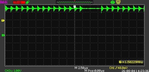
The average voltage is measured to be 3.48V, and the peak-to-peak voltage is measured to be 800 mV. Although the scope is unable to measure the frequency of this ripple, we can read off the scope that the ripple occurs 11 times in (2.50 * 7) us, which gives it a frequency of about 57 kHz.
The power-up reset will now be tested. The following are loaded onto the board:
U2 (MCP130T-315I "3V3 Power Monitor")
D21 ("RESET")
R15 (25k) (note that 25k are not available; 2 x 49.9k will be substituted)
R16 (1k)
From now on, VCC-VEE will be referred to as 'board power' on this page. 48V is applied to board power. D21 flashes on briefly when power is applied, and D20 is steadily illuminated as before.
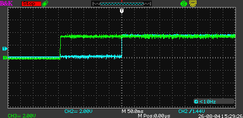
'MCLR' voltage rises shortly after 3V3:
The following are loaded onto the board:
D23 ("CONFIG")
R19 (25k) (Substituted with 2 x 49.9k)
R20 (1k)
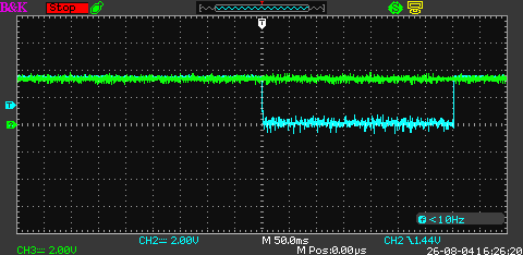
Board power is set to 48V. 3V3 and CFG rise to roughly 3.5V. The "CONFIG" button is pressed and released:
VTM, the transmit power, will be examined next. The following are loaded onto the board:
L4 (SPB06G-05 5V DC-DC Converter)
U7 (SN74LV1T-34DBV)
Q3 (DMP2035U)
L5 (10 uH)
C14 (1 uF)
C43 (100 nF)
R42 (1k)
D22 ("TRANSMIT")
Additionally, 51R is added between 0V and !ON (U7-2).
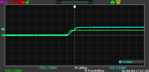
Board power is set to 48V. D22 ("TRANSMIT") remains illuminated. VTM rises to 5V:
Next, a transmit module will be tested. The following are loaded onto the board:
L6 (B3588 Surface Acoustic Wave Filter)
U8 (GALI-3+)
U9 (GVA-92+)
L9 (LFCN1000)
R47 (LAT-2+)
R43, R44, R45, R46 (51R)
C15, C17 (1 nF)
C16, C18 (100 pF)
L7, L8 (22 nH)
P9 (UMCC Connector)
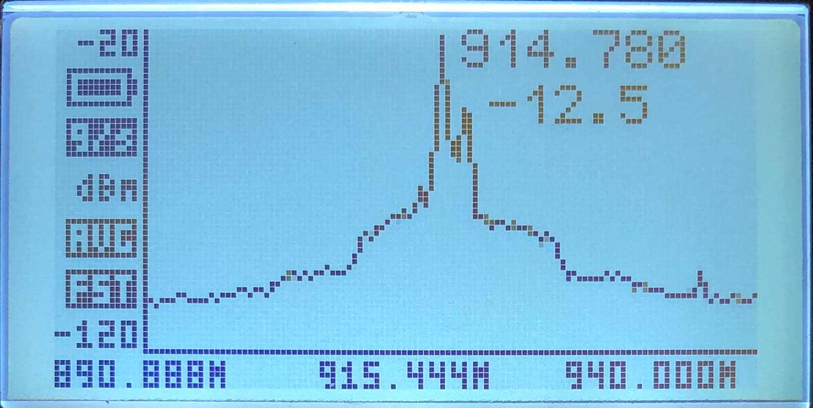
A handheld RF spectrum analyser is connected to P9. This connection is terminated at the spectrum analyser input with a 30 dBm attenuator. Board power is turned on to 48V. The RF spectrum analyser measures a peak of -12.5 dBm at 914.78 MHz:
J3 (mPCIe socket and latch for Detector Module 1) are loaded onto the board.A QC-approved detector module 6BC8 is loaded into J3. Board power is set to 48V. LED1 (Green) and LED2 (Red) on the detector module are illuminated and remain on while power is supplied.
The output of the command transmitter (P9, UMCC) is routed to P1 of the now loaded detector module. This routing includes 60 dBm of attenuation. A function generator is set to put a 0V-3V3 1 kHz square wave on !ON, but this output is not yet powered on. Board power is turned on to 48V. Now the square wave is turned on. The scope trigger is set to rising edge 2V, and test point P on the detector module is measured alongside the square wave:
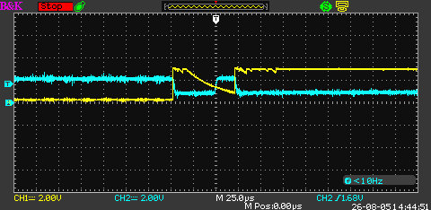
Zooming in on the first Ch2 edge:
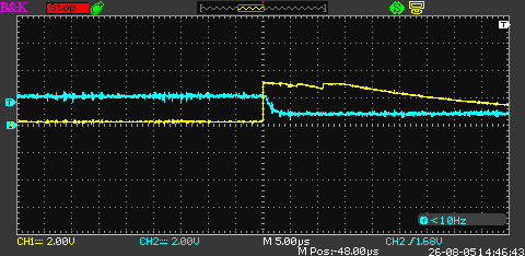
Pressing RUN/STOP on the scope again, the next frame displayed by the scope shows the RF output power (Measured at P) rising when !ON is switched to 0V:
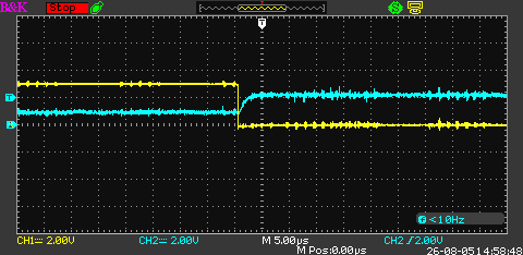
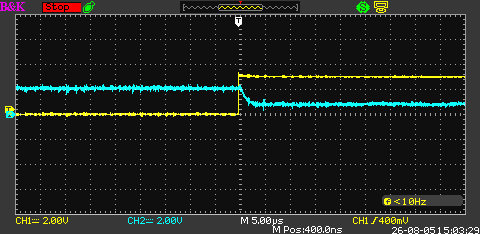
The RF power seems to take about 3 us to reach full power after !ON is asserted.Measuring the fall of RF power as !ON is unasserted, RF power seems to take about 3 us to reach minimum power:
A handheld RF signal generator will be used to examine how the command transmitter output settles when !ON is asserted and unasserted. Command transmitter output is connected through -30 dBm to the RF input of a ZAD-11 mixer. A handhalf RF signal generator is connected to the local oscillator input of the ZAD-11. The intermediate frequency output of the ZAD-11 is terminated with 50R and is measured by the scope. As before, !ON is switched on and off at 1 kHz using a benchtop signal generator.
The handheld signal generator is used to generate +7 dBm 890 MHz for the ZAD-11 LO. Board power is turned on to 48V. The 0-3.3V 1 kHz square wave on !ON is switched on: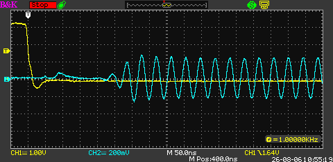
The scope trigger is adjusted to examine the RF behavior during !ON un-assertion (!ON is 0V). The IF signal is seen falling:
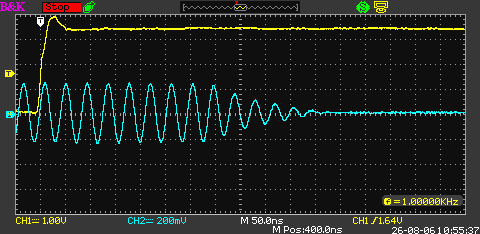
Using a handheld RF spectrum analyser, the power of the command transmitter output was measured while the !ON was being oscillated at 1 kHz. 30 dBm attenuator was attached to RF spectrum analyser input. Command transmitter output power remains with a peak at about 915 MHz, but power fluctuates between -12 and -20 dBm or so (after accounting for the 30 dBm attentuator). Compared to the earlier measurement of 17.5 dBm @ 914.78, this represents a decrease of about 30 dBm power at minimum. In other words, disconnecting the 1kHz square wave from !ON increases the maximum power of the command transmitter by about 30 dBm.
!ON is set to 0V. +10 dBm @ 891 MHz is generated by a handheld RF signal generator, and is routed to the LO input of a ZAD-11 mixer. Command transmitter output is routed through -30 dBm to the ZAD-11 RF input. The IF output of the ZAD-11 is terminated with 50R and connected to the scope:
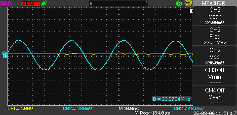
ZAD-11 output is measured to be 23.68 MHz 496 mVpp, yielding a measurement of 891 + 23.68 = 914.68 MHz for command transmitter output frequency.
Next, the behavior of the RF switch will be examined. The following are loaded onto the board:
U16 (PE4259 RF Switch)
C31, C32 (100 pF)
J7, the BNC socket on board edge associated with U16 and the command transmitter which has been tested this far, is connected by a 50R coaxial cable to the RF input of the ZAD-11 mixer. +10 dBm 891 MHz is generated by the handheld RF signal generator, and is routed through -3 dBm to the LO input of the ZAD-11. The IF output of the ZAD-11 is terminated with 50R and attached to the CH2 input of the oscilloscope. Board power is set to 48V. !ON is left asserted (0V) first:
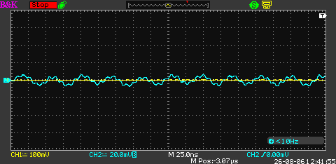
The scope is not able to measure this frequency. The period can be estimated at about 40 ns, corresponding to a frequency around 25 MHz. The smaller oscillation overlaid on the ~25 Mhz is estimated to have a period of 10 ns, corresponding to a frequency of 100 Mhz.
Next, !ON is set to 3.3 Vpp 1 kHz +1.65V offset:
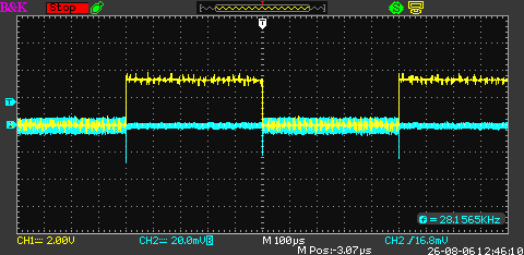
Zooming in on a falling edge of !ON:
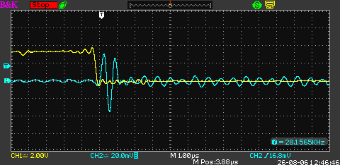
Another zoomed out image of a different !ON falling edge:
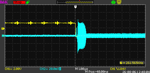
Zooming in on this same frame:
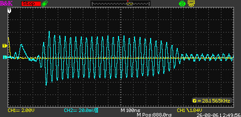
Examining an !ON rising edge:
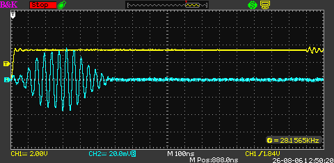
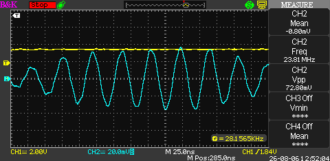
Zooming in to measure the frequency of the signal in the larger-amplitude range, the frequency is measured to be 23.81 MHz:
[18-AUG-2026]Load all parts onto board. Remove U16-20 RF switches. Attach PoE. 3V3, 5V test points are measured at 3.4V, 5V respectively. U7-2 [!ON] and U7-4 [ON] are both measured at 0V. U7-5 and VTM are measured at 5V. Using handheld spectrum analyser, measure RF output power of command transmitters at UMCC jacks (CtrFreq. 915 MHz, range 905-925 MHz, -30 dBm terminator):
P9: 915.630 MHz, -14.5 dBm
P11: 915.450 MHz, -14.5 dBm
P14: 915.630 MHz, -15 dBm
P16: 915.630 MHz, -16.5 dBm
Q3-1 and Q3-2 are measured at 5V.
Notice that U20, U21 have been loaded with SN74LV1T04QDBV, the level-shifting inverter, which is the wrong part. Replace U20, U21 with SN74LVC1G125DBVR.
Remove U7 and replace with SN74LV1T04QDBV level-shifting inverter. Apply PoE. U7-2 [ON] is measured at 0V. U7-4 [!ON] is measured at 5V. U7-5 (power) is measured at 5V.
Measure output power of command transmitters, using handheld RF spectrum analyser (CtrFreq. 915 MHz, range 905-925 MHZ, -30 dBm terminator). Power at UMCC jacks P9, P11, P14, P16 are all negligible.
Attach function generator to ON. Apply 1 kHz 0-3V square wave to ON. When ON is at 0V, !ON is measured at 5V. When ON is at 3V, !ON is measured at 0V.
Apply 0.01 Hz 0-3V square wave to ON. Measure command transmitter output at UMCC jacks P9, P11, P14, P16 using handheld spectrum analyser (CtrFreq. 915 MHz, range 905-925 MHz, -30 dBm terminator). When ON is asserted, command transmitter output is measured as follows:
P9: 915.630 MHz, -13.5 dBm
P11: 915.630 MHz, -14.5 dBm
P14: 915.630 MHz, -14 dBm
P16: 915.810 MHz, -14.5 dBm
Connect command transmitter output through -30 dBm to ZAD-11+ mixer RF-input. Connect handheld signal generator to ZAD-11+ mixer L-input. Apply 920.630 Mhz +2.6 dBm using handheld signal generator. Measure intermediate frequency output (Green), alongside ON (Yellow) and !ON (Blue) using oscilloscope:
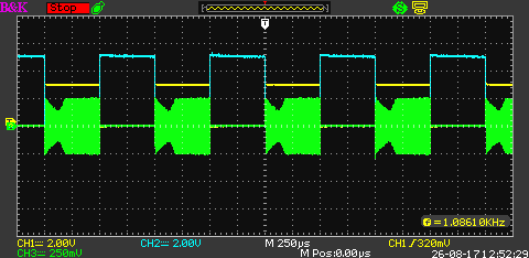
Decreasing the timescale, use the oscilloscope to measure the mixer output frequency and amplitude:
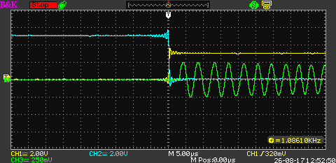
Repeat this process for all four command transmitters, measuring the intermediate frequency output and verifying that command transmitter oscillates while ON is asserted. Measurements at all four command transmitter UMCC outputs is as follows:
P9: 330 mVpp, 5.03 MHz
P11: 320 mVpp, 5.08 MHz
P14: 330 mVpp, 4.93 MHz
P16: 290 mVpp, 4.78 MHz
Note that the intermediate frequency is not completely static during the course of one full ON assertion, but these measurements were taken during the center of an ON assertion, where the intermediate frequency and amplitude do not change much with time.
Load U16, U17, U18, U19 with the RF switch. Apply steady ~3V power to ON with a signal generator on the 'Noise' setting (3.3V mean, 0.5 mV stdev). Measure command transmitter power output at UMCC jacks, using handheld spectrum analyser (CtrFreq. 915 MHz, range 905-920 MHz, -30 dBm terminator):
P9: 915.630 MHz, -21.5 dBm
P11: 915.450 MHz, -21.5 dBm
P14: 915.630 MHz, -22.5 dBm
P16: 915.630 MHz, -24.5 dBm
Using handheld spectrum analyser on same settings, measure command transmitter power output at BNC connectors A1-A4:
A1: 915.450 MHz, -15 dBm
A2: 915.450 MHz, -15.5 dBm
A3: 915.450 MHz, -16 dBm
A4: 915.630 MHz, -17 dBm
Increase the range of the spectrum analyser. The settings are now: CtrFreq. 910MHz, range 860-960 MHz, -30 dBm terminator. Measure the command transmitter power output from the UMCC jacks again:
P9: 914.954 MHz, -18 dBm
P11: 914.954 MHz, -19 dBm
P14: 914.954 MHz, -19 dBm
P16: 915.855 MHz, -21 dBm
Keeping the newly-increased spectrometer range, again measure command transmitter output using the BNC connectors A1-A4:
A1: 914.954 MHz, -12.5 dBm
A2: 914.954 MHz, -12 dBm
A3: 914.954 MHz, -13 dBm
A4: 915.855 MHz, -13.5 dBm
Attach a 48V benchtop power supply to VCC-VEE, and include an ammeter in series with the power supply to measure current drawn by the board. Attach a benchtop signal generator to U7-2 [ON], but do not turn it on.
Turn on the 48V benchtop power supply. The ammeter reads 15.88 mA. Turn off the power supply.
Load an ethernet module onto the board. Turn on the power supply. The ethernet module powers on, and the ammeter reads 34.53 mA. Turn off the power supply.
Keep the ethernet module loaded on the board. Turn on the signal generator to Noise, 3.3V mean, 0.5 mV stdev. Turn on the power supply. The ammeter reads 108.6 mA. Turn off the signal generator. Turn off the power supply.
Remove the ethernet module from the board. Turn on the signal generator to Noise, 3.3V mean, 0.5 mV stdev. Turn on the power supply. The ammeter reads 53.3 mA. Turn off the signal generator. Turn off the power supply.
[19-AUG-26] Repeat board power consumption measurements. Instead of poweringON with the benchtop signal generator, use a wire to connect U7-2 to P1-1. Again connect a handheld ammeter in series with a 48V benchtop power supply.
| Ethernet Module Loaded? | Transmit on? | Current Consumed (mA) |
|---|---|---|
| No | No | 15.88 |
| Yes | No | 40.31 |
| Yes | Yes | 77.5 |
| No | Yes | 53.2 |
[20-AUG-26] Begin assembly of a second A3042B-4 using the A304205A printed circuit board. Load PoE switch components, both DC-DC converters with associated capacitors and inductors, U3-U7 with associated capacitors and inductors, Q3, all diodes and their resistors, and all components of the first command transmitter. Load Q1 belly-up, load J1 PoE socket and A1 BNC socket for first command transmitter.