| Spring-23 | Summer-23 | Fall-23 | Winter-23 | |
| Spring-24 |
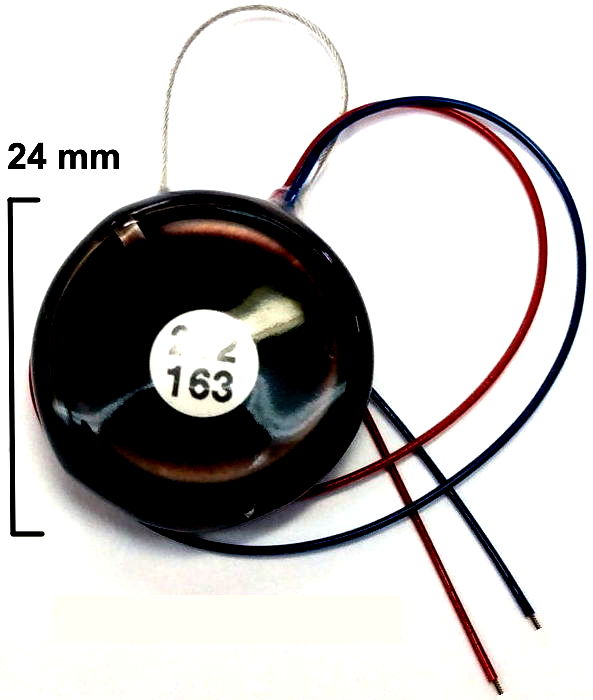
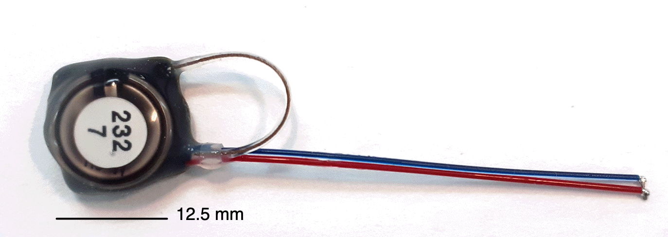
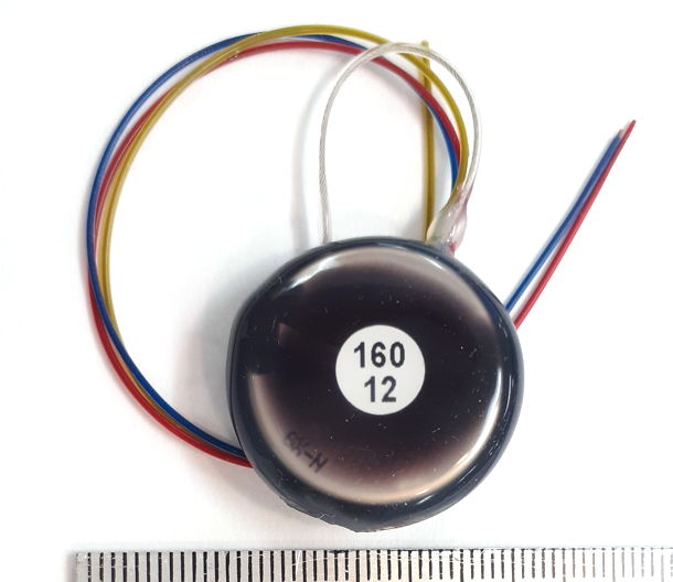
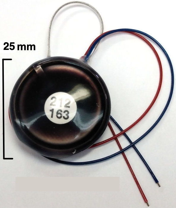
[02-FEB-24] The Subcutaneous Transmitter (A3049) is an implantable telemetry sensor for mice and rats that provides amplification and filtering for up to two independent biopotentials. When equipped with a small coin cell, it is fits comfortably in a mouse. When equipped with a large coin cell, it fits comfortably in a rat. The A3049 operates with our Subcutaneous Transmitter system. We turn the A3049 on and off with a magnet.
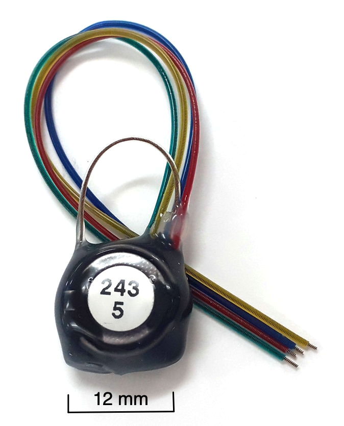
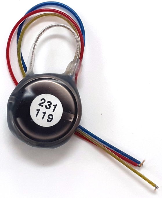
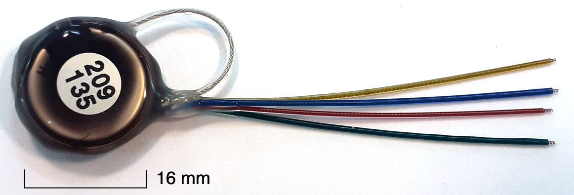
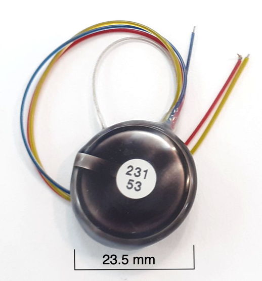
The A3049 amplifier can provide gain of ×100 for frequencies up to 620 Hz. The logic may be programmed to sample at 64, 128, 256, 512, 1024, or 2048 SPS. The low-pass filter may be configured for a corner frequency of 20 Hz, 40 Hz, 80 Hz, 160 Hz, 320 Hz, or 640 Hz. The input high-pass filter provides a corner frequency of 0.16 Hz, but may be removed to give gain all the way down to 0.0 Hz. All versions of the A3049 are equipped with 0.7-mm diameter red and blue leads, and a clear-coated loop antenna. The length of the leads, the battery loaded next to the circuit, the operating life, the termination of the leads, the sample rate, the gain of the amplifier, and the bandwidth of the amplifier all vary from one version to the next.
The A3049 may be configured as a single or dual-input sensor. As a single-input sensor it will transmit one signal on one telemetry channel. As a two-input sensor it will transmit two signals on two telemetry channels. The first channel number will always be an odd-numbered channel. The leads loaded on the transmitter depend upon its "input configuration", as shown below.
| Type | Input Configuration | X+ | X− | Y+ | Y− | Applications |
|---|---|---|---|---|---|---|
| I | Single-Input, X Amplifier | Red | Blue | Omitted | Omitted | EEG, EMG, ECG, or EGG |
| II | Single-Input, Y Amplifier | Omitted | Omitted | Yellow | Green | none |
| III | Dual-Input, Common Reference | Red | Blue | Yellow | Omitted | EEG+EEG |
| IV | Dual-Input, Separate References | Red | Blue | Yellow | Green | EEG+EMG, EMG+EGG, EEG+ECG |
Each transmitter has a label providing two numbers. The first is a batch number, B, the second is a telemetry channel number, N. A single-channel transmitter uses channel N only. A dual-channel transmitter uses channel N for the X input and N+1 for the Y input. In a dual-channel transmitter, N is always odd.
| Property | Specification |
|---|---|
| Volume | 1.2±0.1 ml |
| Mass | 2.2±0.1 g |
| Operating Life | 14 days |
| Battery Capacity | 2000 μA-days |
| Shelf Life | 6 months |
| On-Off Control | magnet |
| Input Configuration | III, Dual-Input, Common Reference |
| Lead Dimensions | diameter 0.7±0.1 mm, length 45±2 mm |
| Lead Terminations | steel coil, diameter 0.45 mm, length 1.0 mm |
| Input Impedance | 10 MΩ |
| Sample Rate | 512 SPS each channel |
| Bandwidth | X: 0.24-160 Hz, Y: 0.16-160 Hz |
| Noise | <10 μV rms |
| Distortion | <0.1% |
| Dynamic Range | 27 mV |
| Resolution | 16-bit |
| Absolute Maximum Input Voltage | ±3 V |
All versions of the A3049 are covered by a one-year warranty against corrosion and manufacturing defect.
[02-FEB-24] The Subcutaneous Transmitter (A3049) can be equipped with a dozen different batteries, any lead length up to 280 mm, several lead diameters, one or two recording channels, a dozen varieties of lead terminations, several types of antenna, and a range of bandwidths, gains, and sample rates. You specify which transmitter you want with a full SCT part number. The part number begins with A2049 and is followed by the primary version letter that tells us the battery we load on the circuit, and the input configuration. Following the letter we have one or two more numbers and letters that specify the sample rate of the inputs. We use the numbers 1-5 to indicate 128, 256, 512, 1014, and 2048 SPS respectively. We use the letter "Z" to indicate that the low end of the frequency response reaches all the way down to 0.0 Hz. After a dash we have a number and letter to specify the length and type of the leads. After a second dash we have letters specifying the electrodes, and after a final dash we have a letter specifying the antenna.
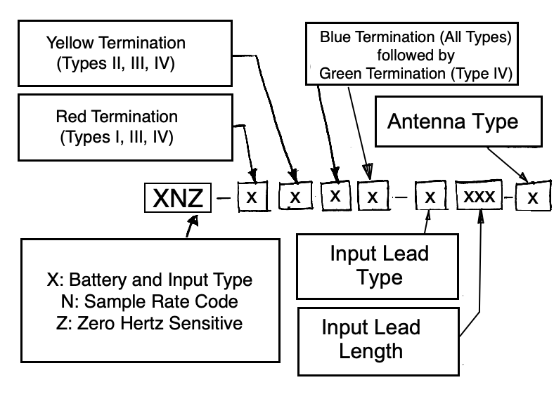
See our Electrode Catalog for a list of terminations and of depth electrodes to which our terminations can be attached. See our Flexible Leads table for a description of our several types of insulated, helical steel leads. See our Antennas table for a description of the various types of antenna we can deploy on our implants. The table below lists the A3028 primary version codes. Battery capacities are usually expressed in units of mA-hr. We convert to μA-dy so it is easier to divide the capacity by the active current and obtain the operating life in days. We give frequency response in Hertz, sample rate in samples per second, and dynamic range of each input in millivolts. The operating life is the minimum time for which a newly-made transmitter will operate continuously. The shelf life is the time the transmitter can remain turned off in storage and still retain 90% of its operating life. Input resistance is either 10 MΩ or 20 MΩ, see Amplifiers.
| Version | Inputs | X | Y | Battery Capacity (μA-dy) |
Volume (ml) |
Mass (g) |
Operating Life (dy) |
Shelf Life (mo) |
|---|---|---|---|---|---|---|---|---|
| A3049W1 | III | 0.24-40 Hz, 128 SPS, 27 mV | 0.16-40 Hz, 128 SPS, 27 mV | 1650 (CR1220) | 1.1 | 2.0 | 34 | 6 |
| A3049W1Z | III | 0.0-40 Hz, 128 SPS, 108 mV | 0.0-40 Hz, 128 SPS, 108 mV | 1650 (CR1220) | 1.1 | 2.0 | 34 | 6 |
| A3049A1 | III | 0.24-40 Hz, 128 SPS, 27 mV | 0.16-40 Hz, 128 SPS, 27 mV | 2000 (CR1225) | 1.2 | 2.2 | 39 | 7 |
| A3049A2 | III | 0.24-80 Hz, 256 SPS, 27 mV | 0.16-80 Hz, 256 SPS, 27 mV | 2000 (CR1225) | 1.2 | 2.2 | 24 | 7 |
| A3049A3 | III | 0.24-160 Hz, 512 SPS, 27 mV | 0.16-160 Hz, 512 SPS, 27 mV | 2000 (CR1225) | 1.2 | 2.2 | 14 | 7 |
| A3049A3Z | III | 0.0-160 Hz, 512 SPS, 108 mV | 0.0-160 Hz, 512 SPS, 108 mV | 2000 (CR1225) | 1.2 | 2.2 | 14 | 7 |
| A3049A4 | III | 0.24-320 Hz, 1024 SPS, 27 mV | 0.16-320 Hz, 1024 SPS, 27 mV | 2000 (CR1225) | 1.2 | 2.2 | 7 | 7 |
| A3049B1 | I | 0.24-40 Hz, 128 SPS, 27 mV | Disabled | 2000 (CR1225) | 1.2 | 2.2 | 54 | 7 |
| A3049B2 | I | 0.24-80 Hz, 256 SPS, 27 mV | Disabled | 2000 (CR1225) | 1.2 | 2.2 | 39 | 7 |
| A3049B3 | I | 0.24-160 Hz, 512 SPS, 27 mV | Disabled | 2000 (CR1225) | 1.2 | 2.2 | 25 | 7 |
| A3049B4 | I | 0.24-320 Hz, 1024 SPS, 27 mV | Disabled | 2000 (CR1225) | 1.2 | 2.2 | 14 | 7 |
| A3049J2 | IV | 0.24-80 Hz, 256 SPS, 27 mV | 0.16-80 Hz, 256 SPS, 27 mV | 2000 (CR1225) | 1.2 | 2.3 | 25 | 7 |
| A3049J3 | IV | 0.24-160 Hz, 512 SPS, 27 mV | 0.16-160 Hz, 512 SPS, 27 mV | 2000 (CR1225) | 1.2 | 2.3 | 14 | 7 |
| A3049F2 | I | 0.24-80 Hz, 256 SPS, 27 mV | Disabled | 3300 (CR1620) | 1.4 | 2.9 | 65 | 7 |
| A3049H2 | III | 0.24-80 Hz, 256 SPS, 27 mV | 0.16-80 Hz, 256 SPS, 27 mV | 3300 (CR1620) | 1.4 | 2.9 | 40 | 7 |
| A3049H3Z | III | 0.0-160 Hz, 512 SPS, 108 mV | 0.0-160 Hz, 512 SPS, 108 mV | 3300 (CR1620) | 1.4 | 2.9 | 23 | 7 |
| A3049K1 | IV | 0.24-40 Hz, 128 SPS, 27 mV | 0.16-80 Hz, 64 SPS, 27 mV | 3300 (CR1620) | 1.4 | 2.9 | 75 | 7 |
| A3049D2 | III | 0.24-80 Hz, 256 SPS, 27 mV | 0.16-80 Hz, 256 SPS, 27 mV | 11000 (CR2330) | 2.6 | 5.8 | 139 | 36 |
| A3049D3 | III | 0.24-160 Hz, 512 SPS, 27 mV | 0.16-160 Hz, 512 SPS, 27 mV | 11000 (CR2330) | 2.6 | 5.8 | 81 | 36 |
| A3049D4 | III | 0.24-320 Hz, 1024 SPS, 27 mV | 0.16-320 Hz, 1024 SPS, 27 mV | 11000 (CR2330) | 2.6 | 5.8 | 43 | 36 |
| A3049E3 | I | 0.24-160 Hz, 512 SPS, 27 mV | Disabled | 11000 (CR2330) | 2.6 | 5.8 | 139 | 36 |
| A3049Q3 | III | 0.24-160 Hz, 512 SPS, 27 mV | 0.16-160 Hz, 512 SPS, 27 mV | 25000 (CR2450) | 4.0 | 8.7 | 184 | 82 |
| A3049Q3Z | III | 0.0-160 Hz, 512 SPS, 108 mV | 0.0-160 Hz, 512 SPS, 108 mV | 25000 (CR2450) | 4.0 | 8.7 | 184 | 82 |
| A3049Q4 | III | 0.24-320 Hz, 1024 SPS, 27 mV | 0.16-320 Hz, 1024 SPS, 27 mV | 25000 (CR2450) | 4.0 | 8.7 | 100 | 82 |
| A3049T5 | I | 0.24-640 Hz, 2048 SPS, 27 mV | Disabled | 25000 (CR2450) | 4.0 | 8.7 | 100 | 82 |
| A3049L4 | III | 0.24-320 Hz, 1024 SPS, 27 mV | 0.16-320 Hz, 1024 SPS, 27 mV | 42000 (CR2477) | 6.0 | 14.0 | 168 | 140 |
For each analog input we specify the bandwidth, sample rate, input dynamic range in millivolts, and channel number offset. In terms of ADC counts, the dynamic range is always 0-65535, as produced by a sixteen-bit ADC. The zero-value of an input is the sample we obtain when we short the two inputs together. The zero value depends upon the battery voltage, VBAT, according to Z = 1.8 V × 65535 ÷ VBAT. The dynamic range is the battery voltage divided by the gain of the amplifier. When we specify dynamic range, we assume VBAT = 2.7 V. When the amplifier gain is 100, we specify dynamic range 27 mV. In practice, VBAT will be between 2.8 and 2.9 V for most of the battery's life, dropping to 2.7 V towards the end of its life.
See below for details of current consumption and how to calculate battery life of new versions of the A3049. By default, we set the top of the frequency range at one third the sample rate. The A3049's low-pass filters provide 20 dB of attenuation at one half the sample rate. Frequencies above one half the sample rate will be distorted by sampling, and so compromise the fidelity of the recording. Because the EEG signal contains less and less power as frequency increases, this attenuation is sufficient to ensure that distortion is insignificant.
[26-FEB-24] The A3049 provides up to four signal inputs: X+, X−, Y+, and Y−. Each of these inputs has a reserved color for its leads: red, blue, yellow, and green respectively. These four leads are present or absent in accordance with each transmitter's input configuration. Whenever the X+ (red) lead is present, it uses the X− (blue) lead as its reference potential. When the Y+ (yellow) lead is present without the Y− (green) lead, the Y+ lead uses the X− lead as its reference potential. When the Y− lead is present, the Y+ uses the Y− lead as its reference potential. When equipped with three leads, the A3049 is a two-channel sensor with a shared reference potential. When equipped with four leads, it is a two-channel sensor with separate reference potentials.

The impedance of X input, as seen at the tips of its electrode leads, is 10 MΩ. When the Y input uses X− as its reference, the Y input impedance is 10 MΩ. When the Y input uses Y− as its reference, the Y input impedance is 20 MΩ. Most transmitters provide a high-pass filter by placing a capacitor in series with the input. The corner frequency of this high-pass filter is 0.2 Hz. When the input impedance is 10 MΩ, the high-pass filter presents a 100-nF capacitor in series with the input, and when the input impedance is 20 MΩ, the series capacitance is 50 nF. When we modify the transmitter to remove the high-pass filter, these capacitors will not be present at the input.
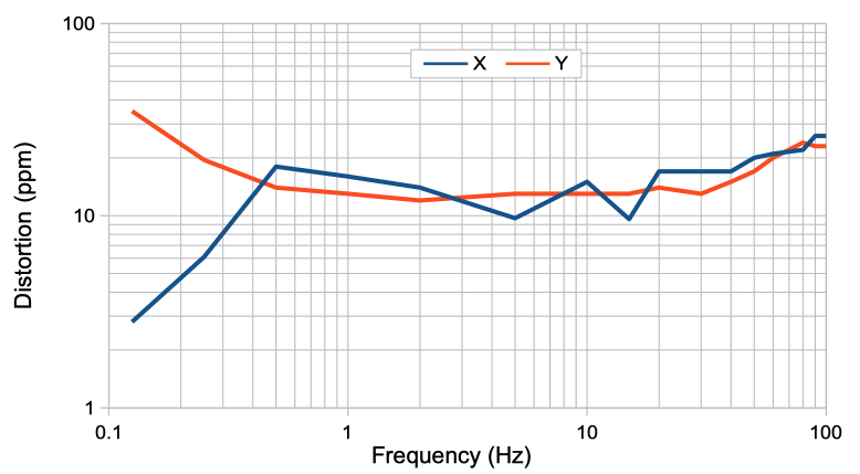
The X signal is supposed to be a measure only of difference between X+ and X−. The average voltage of X+ and X− is the common mode voltage on X, and the difference between X+ and X− is the differential mode voltage. Suppose we apply the same sinusoidal voltage to both X+ and X−. The common mode voltage is the sinusoidal voltage and the differential mode voltage is zero. Under these circumstances, we would like X to be zero, but instead we will see a trace of the common-mode voltage appearing in the X signal. The ratio of the common-mode voltage amplitude and the X signal amplitude is the common mode rejection ratio, or CMRR. The plot below shows how the CMRR of X and Y vary with frequency.
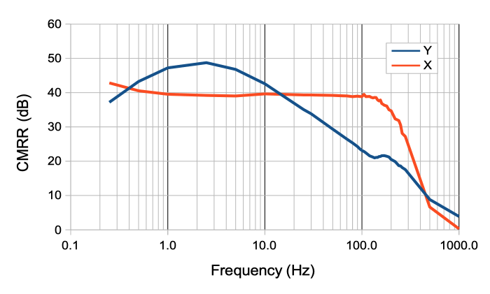
The X-input provides CMRR of 40 dB for frequencies for frequencies below 160 Hz. The signal we see on X will be 1% the amplitude of the common-mode signal we apply to X. The CMRR of the Y-input is >40 dB for frequencies below 10 Hz, but drops for higher frequencies.
The distortion of a signal by our telemetry system is the extent to which it changes the shape of a signal. We apply a 10 mVpp sinusoid to the X and Y inputs of an A3049AV3. The AV3 is equipped with two 160-Hz amplifiers. Input dynamic range is 27 mV. We increase the frequency from 1/8 Hz to 200 Hz. For each frequency, we obtain the spectrum of the signal and measure the power outside the sinusoidal frequency as a fraction of the sinusoidal power using this script. We express the result in parts per million.
The distortion of the X is dominated by random electronic noise. There are no significant peaks in the spectrum outside the fundamenta.
We note that the distortion generated by the A3049 is hundreds of time less powerful than that of its predecessor, the A3028. The A3048 samples the signal uniformly, thus eliminating the scatter noise present in the A3028 signal.
[25-APR-23] Details of the design are available in the following library of design files. Note that all our designs are protected by the GNU General Public Lisence.
S3049A_1.gif: Schematic of A3049AV1[22-APR-24] The following table lists versions of the assembled A3049 electronic circuit, out of which we make the A3049-series transmitters.
| Version | Description | Status |
|---|---|---|
| A3049AV1 | X=0.24-160Hz, Y=0.16-80Hz, U5=U6=MAX4474, C6=L1=1n0, C17=OC, R21=10M | Discontinued |
| A3049AV2 | X=0.24-160Hz, Y=0.16-80Hz, U5=U6=MAX4474, C6=L1=1.0nF, C17=OC, R21=10M | Discontinued |
| A3049AV3 | X=0.24-160Hz, Y=0.16-160Hz, U5=MAX4474, U6=OPA2369, C6=L1=15pF, C17=200Ω, R21=100K | Available |
| A3049AV4 | X=0.24-80Hz, Y=0.16-80Hz, U5=MAX4474, U6=OPA2369, C6=L1=15pF, C17=200Ω, R21=100K | Available |
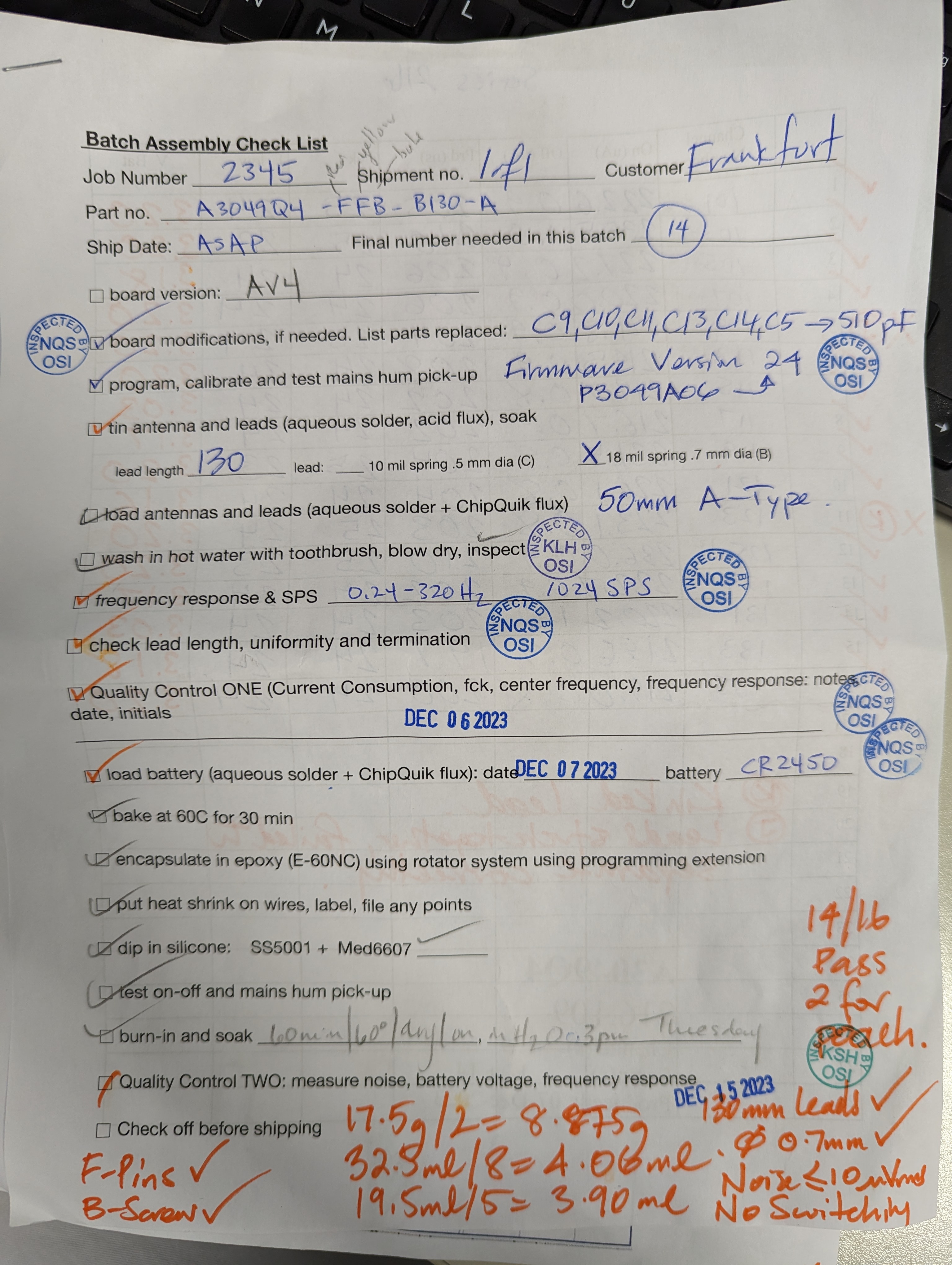
[14-FEB-24] Here we list the electronic circuits we can use to assemble the various types of A3049 transmitter, and the modifications required by that circuit prior to assembly. Roman numerals give the input configuration.
| Configuration | Inputs | Assembly | C7 | R8 | C8 | C9 C10 C11 |
C12 | R15 | C13 C14 C15 |
C16 | R21 |
|---|---|---|---|---|---|---|---|---|---|---|---|
| A3, H3, D3, Q3 | III | AV3 | |||||||||
| A4, H4, D4, Q4 | III | AV3/AV4 | 510 pF | 510 pF | |||||||
| B3, F3, E3 | I | AV3 | |||||||||
| A2, H2, D2, Q2 | III | AV4 | |||||||||
| B2, F2, E2 | I | AV4 | |||||||||
| K1 | IV | AV4 | 3.9 nF | 1.0 μF | 1.0 MΩ | ||||||
| J3 | IV | AV3 | 1.0 μF | 1.0 MΩ | |||||||
| J2 | IV | AV4 | 1.0 μF | 1.0 MΩ | |||||||
| A3Z, H3Z, D3Z, Q3Z | III | AV3 | 1.0 kΩ | 499 kΩ | 1.0 kΩ | 1.0 kΩ | 499 kΩ |
The most complicated modifications are for our 0.0-Hz transmitters, which are those with suffix "Z". In these we must remove the high-pass filter on each amplifier and reduce the ampifier gain to provide greater dynamic range. We replace two or three capacitors with 1-kΩ resistors. We replace two 100 kΩ with 499 kΩ to provide a gain of ×25 instead of ×100, and a dynamic range of 108 mV instead of 27 mV.
[19-APR-23] When we want to mark in our SCT recordings the time at which some event took place, such as the start of a video recording, the moment that a light was flashed, or when an noise commenced, we can use an auxiliary SCT to record a synchronizing signal along with the signals received from implanted SCTs. See the Synchronization section of the A3028 manual for details.
[19-APR-23] See Body Capacitance in the A3019 manual.
[29-APR-24] We equip all our subcutaneous transmitters with CR-series lithium primary cells. The voltage produced by these batteries begins at around 3.2 V, drops rapidly to 3.0 V, remains around 2.9 V for most of the battery's life, and drops rapidly towards the end of life.

The inactive current consumption of the A3049, which is its current consumption when it is turned off, is roughly 0.8 μA at room temperature. When we calculate shelf life, however, we use 1.0 μA for the inactive current consumption, so as to arrive at a conservative estimate of the time it will take for the A3049 to use 10% of its battery while sitting on the shelf. The CR1225 battery has capacity 50 mAhr ≈ 2000 μAdy, so its shelf life is 200 dy = 7 mo.
To obtain the operating life of an A3049 transmitter, we divide the battery capacity in μA-days by the maximum current consumption in μA, and then subtract one day. The subtraction of one day is necessary to account for the twenty-four hours of testing we perform on each transmitter during quality control. To obtain the maximum current consumption of an A3049 transmitter, we use the following relation.
In the above relation, we have 22 μA base current consumption, which powers the logic chip (15 μA), amplifiers (4 μA), and miscellaneous circuits (2 μA). Additional current consumption by digitization and transmission is 0.11 μA per sample per second, or we could say that each sample requires 0.11 μC of charge drawn from the battery. The above formula predicts 50 μA for 256 SPS. The average current consumption of the A3049 circuits is roughly 10% lower than the maximum.
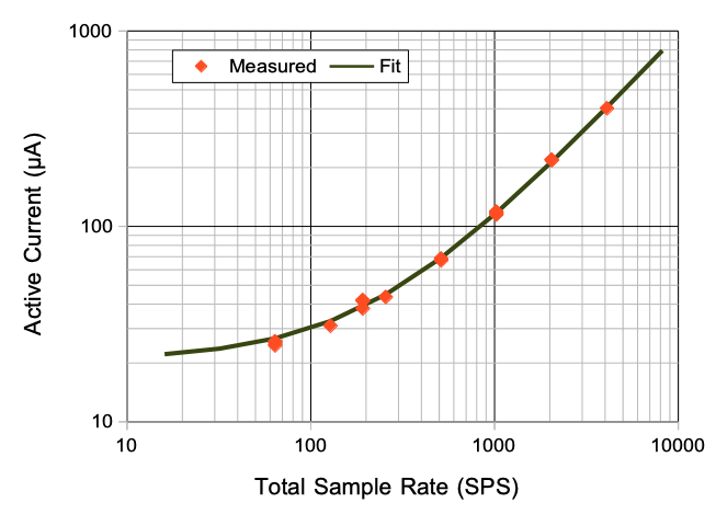
In the table below, we use our formula for maximum current consumption and combine it with the nominal capacity of the batteries we might use with the A3049. The CR1620 is the smallest battery we believe we can load onto the 20-mm diameter circuit. The CR2477 is the largest battery we know for sure that a large adult rat can tolerate.

In each of the above entries, we have divided the nominal capacity of the battery by the maximum current consumption and subtracted one from the result to obtain our guaranteed operating life.
[29-NOV-23] All versions of the A3049 are encapsulated in black epoxy and coated with silicone. The silicone is "unrestricted medical grade" MED-6607, meaning it is approved for implants of unlimited duration in any animal, humans included. The A3049's leads and antenna are encapsulated with dyed silicone, then coated with the same unrestricted medical grade silicone. The only materials the transmitter and its leads present to the subject animal's body are either unrestricted medical grade silicone or stainless steel. When we solder screws or pins to the ends of the leads, there is also solder. Solder reacts slowly with saline, so solder joints must be protected from body fluids by an insulating layer of cement during implantation.
[19-APR-23] Start circuit design. Enhance the second stage of the amplifier so it can provide gain greater than 2.5. We are looking at this circuit: an op-amp with a positive feedback capacitor, which provides two poles for a filter function.

When Ra = Rb, and the capacitors are equal, we must set the gain of the circuit to 2.5 to obtain the second and third poles of our desired 0.5-dB Ripple Chebyshev response. We want to use capacitors of the same value, but we are prepared to use any resistor values. We want to decrease the gain in the first stage, so we can use op-amps with lower bandwidth. We want to increase the gain of the second stage so we can use op-amps that are stable only for gain ≥5, such as the MAX4474. We consider letting the first resistor, Ra, on the left be increased by a factor of α and the second, Rb, be increase by β. To obtain the correct response, we find that αβ = 1 and α is a function of the gain, as shown below.

If we set the gain to 5, we find that we can use 500 kΩ for Ra and 2.0 MΩ for Rb. Furthermore, we can use 2.0 MΩ for R1 and 500 kΩ for R2 and obtain gain of exactly 5.
[23-MAY-23] We receive twenty of A3049AV1. These circuits use the MAX4474 40-kHz amplifier for X and Y. Program with P3049A01. Apply 3-Vpp sweep. In each sweep, we have one of X or Y connected to the sweep through a resistance of 10 MΩ or 100-kΩ, and the other channel open circuit.

The input resistance of Y+/Y− is 20 MΩ, while that of X+/X− is 10 MΩ. The MAX4474 op-amp we use for gain in both amplifiers has a gain-bandwidth product of 40 kHz. The first amplifier stage has gain 20. We predict the bandwidth of the unfiltered amplifier will be 2 kHz. We measure current consumption of three circuits from 64 SPS to 2048 SPS. Intercept is 18 μA + 0.097 μA/SPS.
[26-MAY-23] We vary sample rate and measure active current, see here.
[01-JUN-23] Nathan is applying sparks to the antenna of an A3049AV1 and loading various parts in its antenna matching network (L1, C17 and C6 in S3049A_1.gif) to see if we can reduce the probability of U9, the VCO, being damaged by static electricity. Our spark source is a plasma ball, see here. A direct spark to U9-7 always destroys the VCO. A spark to the antenna with C6 = L1 = 1.0 nF, C17 = OMIT (Network A) usually destroys the VCO, but not always. With C6 = 27 nH, C17 = 200 Ω and L1 = 1.0 nF (Network B), no amount of plasma ball sparking will destroy the VCO, but U9-7 is now connected to VB, which we long ago determined to be a sign of impending failure. After three days running, however, this allegedly damaged transmitter is still running.
With C6 = L1 = 15 pF and C17 = 200 Ω (Network C), no amount of plasma sparking will damage the VCO. The transmitter keeps running, current is normal, and U9-7 has no DC voltage. Nathan sets up the plasma ball and records sparks with a 100-MHz, 2 GSPS oscilloscope equipped with a 500-MHz ×10 probe. We have Network C in place.

The sparks have rapid rising edges, but the peak voltage is attained only after several such steps. In the trace belowl, we see the spark enduring for around 12 μs and reaching 100 V.

Network C is a high-pass filter with corner frequency 50 MHz, so it rejects everything except the jumps in the spark voltage. We compare radiated power with Network C and Network A. We see no significant difference between them. Perhaps Network C is 0.6 dB less powerful than Network A.
[05-JUN-23] We try L1 = 0Ω, C17 = 200Ω, C6 = 15pF, a high-pass filter looking from antenna to VCO with corner frequency 50 MHz. Nathan reports, "This matching network gives a normal power output, but after one shock the transmitter begins consuming 11 mA. This is due to a single shock being able to short the VCO output to VB, allowing for a DC current to flow to ground. This matching network is NOT static proof." We try L1 = 10 Ω, C17 = 27 nH, C6 = 0Ω, a high-pass filter in which the 27 nH interacts with the antenna source impedance. Nathan reports, "After one shock from the plasma ball on the antenna of this transmitter, the transmitter ceases to function. Its current consumption increases to 18mA, indicating to me that the one shock to its antenna permanently damaged the VCO." We conclude that a two-component network that does not cause significant transmit power loss cannot protect the VCO from spark damage. We will use Network C in the A3049BV1.
[08-JUN-23] We receive 80 of A3049AV2 with two 160-Hz amplifiers. Test first circuit, all components loaded correctly. The X-input behaves perfectly. The Y-input has correct gain and frequency response, but is offset upwards. Average value of X for VB = 2.70 V is 43800 (from which we would deduce VB = 2.69 V) and for Y is 56400. We measure with our DVM VC = 0.0 V, U6-4 = −0.2 mV, U5-2 = 4.7 mV, U5-3 = 0.2 mV. Our U5 appears to have an input offset voltage of +4.7 mV, which when multiplied by ×100 gives us a final offset of 470 mV. We also notice a bug in the firmware: the X-channel has the higher of the two channel numbers. We try an A3049AV1 for which X is 47000 and get U6-4 = −03.3 mV, U5-2 = 4.6 mV, U5-3 = 0.2 mV.
[13-JUN-23] We load OPA2369 in place of MAX4471 for U5. The OPA2369 has a maximum input offset voltage of 0.25 mV, compared to 7 mV for the MAX4471. The Y input average drops from 56400 to 40291, compared to 40300 for the X input.
[14-JUN-23] We compare OPA2369 (12 kHz), MAX4471 (9 kHz), and MAX4464 (40 kHz) amplifier gain with no capacitors. The MAX4464 X-channel amplifier output is unstable with no capacitors. With 10-MΩ sweep connected, the output is noisy, but we are able to measure amplitude. The MAX4464 is operating with gain ×5 in the second stage, which is the minimum gain for which it is stable. The other two op-amps produce a stable output.

The bandwidth is limited by the ×20 gain of the first stage. We expect bandwidth 12 kHz ÷ 20 = 600 Hz for the OPA2369 and 9 kHz ÷ 20 = 450 Hz for the MAX4471. We observe 3-dB bandwidth 400 Hz for both. We must load the OPA2369 for the Y-channel to avoid large DC offsets in the amplifier output. Our Y-amplifier will support SCT bandwidths up to 320 Hz at 1024 SPS. With MAX4464 loaded in the X-amplifier, we expect bandwidth 2 kHz, permitting sample rate 4096 SPS. Our A3049AV3 and AV4 circuits will support dual-channel up to 1024 SPS or single-channel up to 4096 SPS. If we want faster dual-channel transmitters, we must revert to the OPA2349 70-kHz amplifier, of which we have one thousand on the shelf.
[15-JUN-23] We load OPA2349 for U5, replacing an OPA2369, and find that the Y-amplifier output rises from 44 kcount, which is the same value we have for X, to 48 kcount because of the OPA2349 input offset voltages. We measure sweep with 240 pF capacitors loaded in the amplifier. We do the same for MAX4474 and MAX4471. The MAX4474 is stable with 240 pF. The MAX4471 provides greater bandwidth with 240 pF.
[27-JUN-23] We have twenty-three A3049A3-AAA-B200-B made with the A3049AV2. The long leads on these devices pick up lots of mains hum and other noise. The Y-channel offsets generated by the MAX4474 are excessive. We provide 2.64 V to each device in turn, place lead tips in water to reduce mains hum, and measure the average value of X and Y, then calculate the equivalent offset voltage across U5-2 and U5-3. Half of the circuits we could allow to proceed without modification, but the other half require that replace U5 with OPA2369. We resolve to replace U5 on all of them.

When both amplifiers are saturated with mains hum, current consumption of the A3049AV2 programmed as 49A3 rises from 125 μA to 155 μA. With only one saturated with mains hum, increase is 15 μA. When we perform the same test on an A3028KV2, we see increase an increase of only 5 μA.
[28-JUN-23] We replace U5 on two of our A3049A3-AAA-B200-B. With a battery as power supply, X and Y have the same average value within a ±500 μV. But when we connect an external power supply, we see the Y input of every circuit dropping down, sometimes saturating at zero, sometimes with a constant negative offset with respect to X. The X input remains centered where we expect it to be. We connect probes to Y+, X+, and Y−, grounding them to VC, and see the following.

Here we see the effect of the long leads: Y− has far less noise than Y+. The noise is around 300 kHz, far above the 12-kHz bandwidth of the OPA369 that buffers Y−, and of amplitude 100 mVpp. With our probes disconnected, current coming from bench-top power supply, and the three long leads loaded on X+, X−, and Y+, we see Y offset by −14 kcnt (−5.6 mV) with respect to X. We remove the Y− lead and now Y is offset by +0.6 kcnt (+0.2 mV). Reconnect Y+ and power with battery, Y offset from X by −0.4 kcnt (−160 μV).
We replace U5 on all 23 of our A3049A3-AAA-B200-B. Half of them have X and Y within 500 cnt. But the other half have extreme and fluctuating baseline value of Y. As we change the noise or mains hum on the inputs, the baseline of Y can shift. The baseline of X never shifts. We examine U6-1 and U6-3. We sometimes see pulses at 1 kHz on U6-3. We sometime see a −20 mV offset on U6-1. We replace all R21 = 10MΩ with R21 = 100 kΩ. We wash and dry. None of the circuits show noise on U6-3 nor offset on U6-2. Every Y is within 500 cnt of X. Noise on both inputs is sinisoidal mains hum of equal amplitude and matching phase. Update S3049A_1 so that R21 = 100 kΩ, U5 is OPA2369, C6 = L1 = 15 pF, and C17 is 200 Ω.
[30-JUN-23] With latest measurements, current consumption of the A3049AV2 has slope 0.095 μA/SPS, intercept 20.0 μA. Compare to latest A3048AV1 measured slope 0.106 μA/SPS, intercept 16.1 μA.
[03-JUL-23] We receive 99 of A3049AV3 and 105 of A3049AV4. We take three of each type to test. These boards have MAX4474 for U4 and OPA2369 for U5. In place of L1 and C6 they have 15 pF, and for C17 they have 200 Ω. The AV3 has 160-Hz corner frequency, the AV4 has 80-Hz corner frequency. Each board is labelled with an index and version. We program as A3049AV3 and check frequency response, power output, and channel offset.

When we first program 180AV4, the Y channel offset is 5.9 mV. We see U6-3 at −10 mV and U6-1 at −8 mV. Circuit 066AV3 has Y offset 2.6 mV. We load R21 with 1 MΩ on both these boards and see the offsets drop to 0.7 and 0.9 mV respectively. When we load R21 with 100 kΩ, the offsets drop further to 0.12 mV and 0.48 mV, which is consistent with the ±0.75 mV input offset voltage of the OPA369. We resolve to replace R21 with 100 kΩ for all dual-channel transmitters that use VC as a common reference. When we use Y− as the reference for the Y-channel, we will replace R21 with 1 MΩ and see what happens.
[05-JUL-23] We have a batch of 23 of A3049A3-AAA-B200-B encapsulated. Frequency response and X-Y offsets are all fine, but noise in the Y channels is 20-30 μV consisting of single-sample spikes of up to 80 μV. The X-input noise is 10 μV. We trace this to a firmware timing error, combined with the Y-amplifier op-amp OPA2369 being slower than the X-amplifier op-amp MAX4474. We need to give the amplifiers time to drive the ADC input in advance of the next sample. We fix the problem by increasing the minimum number of clock ticks between selecting a new channel and the ADC conversion. We increase the End Clock Offset from 1 to 7 and measure noise on X and Y. We measure crosstalk also, by applying a differential mode signal to the other input of amplitude 15 mVpp, and measuring the ratio of the the test input amplitude to the other input's amplitude.

We enhance the firmware so it applies an offset chosen to suit the sample period. For 4096 SPS, the offset is only 3, but for lower sample rates, we increase the offset until for total sample rate 512 SPS and lower the offset is 15. In a batch of A3049H2, noise on X and Y is around 20 cnt.
[06-JUL-23] We re-program all 28 of A3049H2 with our new firmware. Total sample rate is 512 SPS, so we have ECK offset 15. After re-programming, noise on X and Y with leads in water settles down to around 12 cnt rms, or 5 μVrms. We study sampling noise with an A3049AV3.

We drive CONVST LO while we read out the ADS8860. We drive it HI to initiate conversion. In our latest firmware, we keep CONVST LO until we are done with RF transmission. Driving it HI as soon as all ADC readout is done, before the RF transmission is complete, works just as well.

In the longer view, we see 20-mV sampling ripple on the analog power supply, VA. Right now we are using ECK Offset to give us time for the X and Y amplifiers to settle after selection with our analog switch. We try switching immediately after conversion, with the falling edge of ACTIVE, or the falling edge of Delayed ACTIVE, or the falling edge of Delayed Delayed ACTIVE. But neither offers lower noise.

[07-JUL-23] We are trying to understand why it is that switching between X and Y with U7 at !ACTIVE results in noise on X and Y, while switching at ECK does not. We synchronize CONVST with TCK, so that it goes low at the start of serial readout and goes hi after the last RF bit has been transmitted. We start with switching on ECK, inputs open-circuit. We switch on !ACTIVE, inputs open-circuit and see the spectrum of "antenna noise", which is the noise we get from a transmitter in water with a broken ground lead. We short the X and Y inputs to ground and measure the spectrum again.


Instead of !ACTIVE, we try !DDA, which is a rising edge 60 us after !ACTIVE. We see the same open-circuit noise. We suppress transmission scatter, switch on !ACTIVE and the antenna noise vanishes. We restore transmit scatter, and add another CONVST low pulse two CK periods before ECK, so we are now converting twice during each sample period: once immediately after readout, another time before ECK. Antenna noise vanishes. Current consumption for this 1024 SPS device increases from 121.6 μA to 126.2 μA when we add the extra sample. We shorten the secondary CONVST pulse with the help of !CK, but this does not reduce the current consumption. We return to just one CONVST pulse, but we set it equal to !ACTIVE. Current is 121.3 μA. We examine the output of the switch, which is U7-5. We trigger on SEL, which goes HI to select X, LO to select Y. We look at CONVST as well. We are running at 512 SPS per channel.

We see AINP jump down upon selection of X, recovering with two bounces in 100 μs. Another negative bounce during ADC sample and hold, recovering in 100 μs. This X-signal is provided by the 40-kHz MAX4474. We see AINP jump down again upon selection of Y, but this time the recovery consists of only one bounce and takes 200 μs. The same thing happens after conversion. The Y-signal is provided by the 12-kHz OPA2369. We want to allow sufficient time after switching before conversion, which appears to be around 200 μs, or seven CK ticks. One way to do that would be to switch 30 μs after conversion. If we switch synchronously with conversion, the switching is scattered, and we see noise induced on our open-circuit inputs. We look at the path of SEL from its source on U11 to its destination on U7 and we note that it passes beneath both amplifiers, threading its way between resistors in the top layer. We speculate that the edges of this signal induce noise in the amplifier input, but we note that SEL does not pass close to the amplifier inputs XP and YP. When we short the amplifier inputs, this SEL-induced noise disappears.
[18-JUL-23] Measure distortion in the X and Y inputs of the AV3. The distortion is dominated by transmission scatter for frequencies above 10 Hz.
[19-JUL-23] Eliminate scatter noise in firmware P3049A05 by adding a pulse on CSS during the last CK period during the sample period. We synchronize CSS with TCK during the serial readout, and this readout pulse remains shorter than the ACTIVE pulse. We now have two conversions per sample period and one readout. Current consumption of the A3049A3, with 2 × 512 SPS rises from 116.7 μA to 118.9 μA, or 0.002 μA/SPS, which is negligible compared to our existing 0.11 μA/SPS. Total harmonic distortion now remains below 20 ppm and is caused only by random noise.
[01-AUG-23] Discover bug in P3049A05, whereby for versions 21 and 31 and base id 87 we get x_id 87 and y_id 216, due to top bit of ID being inverted for second channel. We conclude this is an ABEL compiler bug. We work around the bug by calculating the completion code, cc, directly from x_id and y_id in our sample counter state machine, rather than from the intermediate id nodes, which are eliminated later by the compiler anyway.
We have encountered five A3049AV3/4 assemblies with U1 tilted on the board and one of the pins not soldered. The picture below is an example. We reflow the joints and the component sits properly on its footprint, circuit works.

[03-AUG-23] We have our first batch of A3049K1 with wires loaded, ready for QC1. The K1 is a dual-channel transmitter with 128 SPS and 0.24-40 Hz on X for EEG and 64 SPS and 0.16-80 Hz on Y for EMG. Current consumption is 38-42 μA. Noise is 5 μV on X and 6 μV on Y.
[10-AUG-23] We drain three of each of four types of battery over the course of a week: CR1025, CR1225, CR2330, and CR2450. We drain each battery with a resistor. Twice a day, we measure the battery voltage, disconnect the resistor, and measure the battery voltage again. For each type of battery we use a fixed resistor. We model the battery as a voltage source in series with a source resistance. We calculate this source resistance from our open-circuit and loaded battery voltage measurements, and our knowledge of the load resistance. We define the nominal drain current as the nominal battery voltage divided by the drain resistor. We take the nominal battery voltage to be 2.7 V. We plot the source resistance versus charge drained from the battery.


The capacity of these batteries decreases with drain current. The CR1025 capacity of 30 mAhr, for example, is specified for a drain current of 0.05 mA. The capacity decreases as drain current increases. Our CR2450 drain resistor was 630 Ω. The CR2450 data sheet specifies capacity only for loads 1 kΩ and higher. The plot below implies that the capacity for our 630 Ω load could be as low as 300 mAhr, and indeed this is what we see in our drain plots.

We are draining all our batteries at higher than their maximum recommended rate. The effective source resistance remains roughly constant during the drain. One of the features of our A3048 and A3049 transmitters is the 2 mA burst of current they need when we turn them on. We conclude from the above study that, if a battery can power up an A3048 or A3049 when it is fresh, then it can do so for its entire operating life.
[11-DEC-23] We have three A3049J3-AAAA-C40-D. The Y+ input is 100 nF and 10 MΩ. The Y− input is 100 nF and 1.0 MΩ. If we ground Y−, our low-frequency cutoff is 0.16 Hz. If we ground Y+ out cutoff is 1.6 Hz, as we observed today.

In future, we will load C16 with 1.0 μF in order to bring the cut-off down to 0.16 Hz for both devices. We adjust our modification directions accordingly for J and K series devices.
[14-DEC-23] We study the cross-section of an A304901A PCB sent to us by the fab house. With a microscope and graduated loupe we obtain the photograph below.

Nathan writes, "I imaged the cross section of the A3049 PCB and measured it using the thickness of the board (31 mils) as a reference frame. I've attached the image I measured. I measured each of the copper layers to be roughly 1.3 mils. The first layer (from left to right) inside of the PCB is roughly 4.3 mils from the top of the board. The next layer is about 6.2 mils from the layer above it. The middle two layers are separated by about 5.3 mils. the furthest right layer is roughly 6.3 mils from the layer to its left. Lastly, the rightmost layer is about 4.3 mils from the bottom side of the PCB. All of these measurements add up to 31.3 mils, 0.3 mils off of what I measured the thickness to be with calipers (31 mils). A diagram of the PCB thickness would look something like this: Top of PCB(4.3 mils [1.3 mils Cu] 6.2 mils [1.3 mils Cu] 5.3 mils [1.3 mils Cu] 6.3 mils [1.3 mils Cu] 4.3 mils) Bottom of PCB."
[19-DEC-23] We have A202_115 and A202_119, both A3049A3, that we poached in acetone and ethanol respectively for three days at 60°C. No115 is visibly enlarged and softened by the acetone poach. No119 is slightly discolored. Both devices turn on and transmit. We turn off and place both in water for one day at 60°C, each in its own container. Upon opening the containers today, we smell acetone in the container of No115 and ethanol in the container of No119. No115 will turn on. No119 does turn on. The silicone of No115 is now lumpy and deformed by sub-surface fissures. The silicone of No119 is slightly deformed after the same fasion.


Aside from its unattractive appearance, the deformed silicone permits more rapid corrosion of the battery casing, as we can see below.


We have two A3049Q4 transmitters that soaked for four days, ran in water for one day, and passed QC2 easily, with the exception of 2/16 whose only flaw was kinked leads. These two we poach in water at 60°C. After three days, Y of one is saturating near the bottom of its range. After four days, Y of the other is doing the same. We call this the bottom-side flat-lining problem, and we distinguish it from a saturation near the top of the range, which will be top-side flat-lining. We bake both in our oven for an hour. The bottom flat-liniung persists. We turn on and off, effect persists. We remove silicone and epoxy around U6 on both devices. The effect persists. We connect a scope probe to VC and find U6-4 is saturated at VA in both devices, and U6-3 is close to 0V.

We dissect No123 further, until we reveal all components around U6 and expose all its pads. While dissecting, U6-4 drops back to VC, so that Y re-appears, then returns to VA, so that Y flat-lines. We short U6-3 to VC and to VA and find this sometimes restore the op-amp to proper function in both devices. At one point, both Y-signals are working. We place both transmitters in our Faraday enclosure with a sweep and they respond perfectly for half an hour. Later, while examining No123, Y starts saturating soon after we connect a ground clip to VC. We notice this effect at least twice, but it is not repeatable. With ground clip attached to VC, we measure U6-1 = 0.02 V, U6-2 = −1.80 V, U6-3 = −1.64 V, U6-4 = 1.18 V, U6-5 = 1.18 V. We measure R21 = 100 kΩ, R22 = 2.0 MΩ, R23 = 100 kΩ. We have 28 μA flowing through R23 and 0.8 μA flowing through R22, and 28.8 μA entering U6-3, the inverting input. We now find we are unable to restore Y by any means. Whatever we do, U6-3 immediately drops to −1.64 V afterwards, whereupon U6-4 goes to VA. We apply flux and clean up all the pads, wash, and blow dry. We still have U6-3 at −1.64 V. We replace U6. We find plenty of epoxy under the leads, suggesting a good fill during encapsulation. With new U6, Y amplifier performs perfectly. We check our source for OPA369: all purchased from DigiKey. We consult our recording of all 16 Q4 transmitters during QC2, M1702650377.ndf. All Y-amplifiers are performing perfectly in the five-minute recording.
[20-DEC-23] We are unable to invoke latch-up in either No109 or No123 by connecting our ground clip to C. Recall that U6 in No123 is new, while U6 in No109 is the original. When we connect our clip, we see 20 kcnt of mains hum, and Y in No109 drops by 10 kcnt, while Y in No123 remains the same. We record from No109 and No123 in our Faraday enclosure. They are clipped into our 100-kΩ source, but we have no signal applied.

The Y-input of No109 is drifting and spiking, but it is not flat-lining. The drifting and spiking of Y in No109 is sustained through a half-hour recording.

We remove epoxy from around U6 on No109, exposing all five of its pads. Wash, blow dry, and bake. The drift and spiking are gone. We connect ground clip and see no offset in either Y-input. We connect 10-MΩ sweep, response is perfect, leave running. We put flux on no109 U6-2 and U6-3 so as to introduce a high-impedance connection. We see Y drift down and become noisy. We do not see the original problem recurring: U6-3 at −1.64 V and U6-4 saturating at VA.
Claim: The rumble and spikes in No109 are due to a variable 20-MΩ connection between U6-3 and U6-2 that we introduced when we dissected the circuit with flux and washed with water. They are not related to the original failure of the transmitter during poaching.
Claim: The bottom-side flat-lining problem is consistent with an intermittent 5-kΩ connection between U6-2 (0V) and U6-3 (IN-). When this hypothetical connection is closed, 30 μA flows from U6-3 at −1.64 V to U6-2 at −1.80 V. When the connection is open, the op-amp behavies perfectly.
We look for cavities inside the OPA369 encapsulation. Sam reports, "Four OPA369s were dissected. The first one was cut in half, breaking off a copper track, revealing what looks like a cavity underneath it. The other three were sanded down. No cavities were to be found when the top, bottom, and sides were sanded."
We take a fresh circuit and lift U6-1. The amplifier saturates near 0V and Y flat-lines at the top. We reconnect U6-1 and lift U6-3. The amplifier saturates at VS and Y flat-lines at the bottom. But the junction between R22 and R23 is at VS too. The bottom-side flat-lining problem that arose during poaching is not consistent with an internal wire bond break in the op-amp.
Nathan writes, "Per your request I sparked the leads of an A3049 transmitter we had on the shelf with a plasma ball. I tried sparking the blue lead around 30 times and never achieved a latched state. I sparked the positive input leads on the two channel transmitter and managed to get both channels latched, saturated to the bottom rail. Most of the time I tried sparking the leads of the transmitter it would either do nothing or turn the transmitter on/off. When I did manage to get both channels flatlining the problem was solved by turning the transmitter off and then on again." The dual-channel flat-lining Nathan observed was what we see when the ADC latches up.
The U6-2 and U6-3 pins are adjacent to one another and near the VB battery pad, where we solder the positive battery tab. They get covered in no-clean, water-soluble flux during assembly, then washed multiple times, cleaned and inspected by Kirsten, see batch sheet. The likelyhood of these boards being dirty is small. If the problem were flux-induced corrosion, the corrosion short would not turn on and off abruptly multiple times in response to electrical signals.
We consider corrosion in the circuit board forging a connection between U6-3 and 0V. But the U6-3 network is entirely on the bottom side of the board, and there are no vias carrying 0V aywhere near the U6-3 network. The only 0V nearby is U6-2. When we clip the battery extension, we might short VB to YP or YN with our clippers. At that time, the circuit is almost certainly turned off. We connect 3-V pulses to U6-1 and U6-3 on No109 when the device is on and when it is off, multiple times. We connect a ±3-V, 10-Hz square wave multiple times to both pins when on and off. The transmitter continues to function perfectly. We leave No109 running in a dry petri dish at 60°C.
Continue poaching of No115 and No119 in water. No119 still working and looks much the same. No115 still won't transmit. We see circular cavities under the silicone. We dissect and find current is fluctuating around 90 μA, but transmissions are not being received.
[21-DEC-23] No109 running fine after over-night baking.
Claim: We failed to clean the flux out from under U6 in this batch of Q4 transmitters. Flux, condensation, heat, and electrical potential gave rise to metallic migration between U6-2 and U6-3, culminating in a low-impedance connection that dragged IN- almost to 0V. This metallic connection is intermittent once disturbed. It exists on the circuit board beneat the epoxy and component body.
We write to our customer and tell them we believe their Q4s will fail after thirty days implanted, and inform them that we will ship a replacement batch to them the first week of January.
[27-DEC-23] Nathan writes, "Per your request I've been sparking the input leads of an A3049 transmitter I found in the sample tray by the faraday canopy, A202.119. I sparked each of the blue, yellow, and red leads 50 times individually while the transmitter is off. It is important to note that the transmitter would frequently change its on/off state when sparked on its input leads. Therefore, not all 50 shocks were applied when the transmitter was off, it was more like half of those 50 shocks were during the transmitter being off. Despite being shocked 50 times on each lead and turning on and off through being shocked the transmitter's analog response looked just as perfect as before I shocked it at all. No noticeable changes were observed by shocking the input leads."
[03-JAN-24] We damage an A3049Q4 while spot-welding its battery tabs. Sparks flew out from on of our welds. The transmitter no longer transmits. Remove battery. Current consumption 42 mA. We remove one component after another, until only U1 and U2 remain. There are no passives left. We remove U2 and current drops to normal: 0.8 μA.
[05-JAN-24] We find, after encapsulation and coating, that a Q4 we previously had to replace tabs on after sparking spot-welding, will not turn on. We dissect and find that U2 is drawing 4.9 mA.
[12-JAN-24] Nathan reports, "When wielding a battery on a Q4 transmitter we discovered that somewhere in the spot wielding process the transmitter was damaged. To study this phenomenon we looked at the power supply voltage on the transmitter with a scope probe while I was wielding. We notice the voltage could vary by +/- 7V from the initial battery voltage during the wielding pulse (roughly 20ns). To avoid this damage we make a molex compatible through hole 5.6V zener diode (reverse biased) with 50 ohms in series that could be loaded on the transmitter across the power supply while loading batteries. With the diode loaded, we spot wield a CR2450X Murata battery to an A3049A3 transmitter and wielded the negative side as many times as possible in an attempt to spark the negative side and cause ripples in the power supply. After the battery became too hot to touch we remove it and measured the circuit's current consumption. This transmitter showed signs of damage (I_on= 7.5mA) and after removing some parts we determine that U1 is damaged. We replace U1 and U2, and this time we try putting a 5.6V zener diode (reverse biased) across the power supply without any resistance in series. We try to damage the circuit in the same manner while loading a CR2450X battery and notice that the current consumption remains the same. This indicates that the spot wielder induces roughly more than 100mA through the transmitter circuit for about 20ns. In the future we will wear gloves and place the 5.6V zener diode across the power supply when loading batteries to avoid damage."
[18-JAN-24] We take ten CR1225 batteries and weld tabs to them with three spot welds on each tab, waiting four seconds between each weld to allow the battery to cool. We load each battery with 10 kΩ soldered between its tabs. The batteries are numbered 1 to N. We spot-weld the negative tab an additional 3*(N-1) times, waiting one second between welds, so that the 10th battery receives 27 welds. We measure battery voltage versus time starting one hour after the final welds.

If we consider failure to be when the voltage drops to 2.0 V, which is the definition used in the Renata CR1225 data sheet, operating life is 172-191 hr with no correlation to the number of spot welds. Assuming 270 μA average current we have approximate capacity 46 mAhr to 52 mAhr. The Renata CR1225's nominal capacity with 10 kΩ load is 43 mAhr.
[22-JAN-24] We have our first working LWDAQ Function Generator (A3050). With it, we measure the sweep response of an A3049Q4 to sine, triangle, and square waves using our new SCT Check tool.

[22-JAN-24] We have been poaching silicone in water, acetone, and vinegar. Nathan reports as follows. "When we received transmitters used by Yunan, we noticed some of them appeared to have visible silicone damage and smell of acetone when being poached in water. In an attempt to recreate what caused that damage, we poached samples of 5001 silicone in various substances at 60 degrees centigrade. We measure a disc of 5001 silicone's mass to be 2.125g before we poach it in water and 2.133g after we poach it in water. We measure another disc of 5001 silicone's mass to be 3.939g before we poach it in Ethanol and 3.905g after. We measure a disc of 5001 silicone's mass to be 3.305g before we poach it in acetone and 4.166g after poaching. After allowing the disc to sit out in open air for a few minutes we notice the mass drop down to 3.358. This indicates to us that the disc being poached in acetone soaked up roughly 26% of its mass in acetone and lost much of that acetone to evaporation when taken out of poaching. We then place that same disc that was poached in acetone in water and poach it again. Taking out the disc we notice that the water and disc smell of acetone telling us that some of the acetone was dissolved in the water. The disc also becomes deformed and wrinkled as though it underwent expansion and shrinking. Lastly, we poach a disc of 5001 silicone in vinegar. Before poaching its mass is measured at 3.722g and after poaching its mass is measured as 3.719g. The disc of silicone did not soak up any vinegar during poaching so we moved the disc to water to see if it deforms. We poach the disc in water for a day and observe a slight scent of vinegar that was dissolved into the water but the disc is not deformed or wrinkled at all. If somebody were to remove dental cement from one of our transmitters, vinegar is much less likely to cause damage to the silicone on the transmitter than acetone."
[27-FEB-24] Kirsten completes a study of the effect of acetone and water on our round transmitter labels. "I conducted a simple study on the deterioration of the transmitter stickers after we received some transmitters back that had been severely distorted. I was trying to replicate that distortion to understand what might have happened to those transmitters. I made two jars which could go into the oven. The 60 degree centigrade oven increases aging time. The first jar contained acetone. The second jar contained water. I placed three stickers in each jar, and placed the jars in the over for two weeks. At the end of two weeks, I compared the poached stickers with the ones that had never been in any liquid. I found that the stickers in water had very little change to them. Perhaps the ink appeared slightly less thick on the water soaked set. On the stickers that had been in acetone, the ink appeared noticeably fainter. And also, the adhesive had dissolved. However, I did not observe the same kind of distortion I was trying to replicate on the returned transmitters."

[28-FEB-24] We measure frequency response of four A3049E3 before and after encapsulation. We plot on the same graph.

[22-MAR-24] We observe a transmitter poaching with VB=2.90V one day and fail the next. We dissect to find VB=1.2V and active current consumption with external source is 40 uA. If a short brought down the battery voltage, where is the short now? If it was a temporary short, why do we see no sign of it now? We measure current consumption for falling and rising battery voltage. Nathan reports, "We measure the current consumption of an A3048S2 transmitter with respect to its battery voltage. First, we start by applying 3V and decreasing the voltage down to zero while measuring current consumption and notice that the device stops transmitting around 1.8V. Then, we start at 0V and increase the voltage applied on the circuit to 3V noting that the device begins to transmit around 2V."
This behavior will cause a transmitter to drain its battery if for a brief period a corrosion short develops and drags the battery voltage down to 1.8 V. Today we discover that one of a batch of ten A3049J2 devices latches up when we turn it on, provided it has sat in the off state for ten minutes. We dissect and find VB 2.9 V, Ion 70 μA, Ioff 0.9 μA.
[10-APR-24] We study the startup current consumption of the A3048, A3049, and the discontinued A3028. See Nathan's report, from which we extract the following figure.

The startup current consists of 7 mA for 5 ms followed by 3 mA for 120 ms. We believe the ADS8860 is responsible for the 3 mA for 120 ms. The A3028, which uses the LTC1865L in place of the ADS8860, shows no sign of any startup current other than an initial 7 mA for 5 ms, which we believe is current rushing into the power supply decoupling capacitors. it is the 3 mA for 120 ms that can cause the circuit to fail to power up when the source resistance is greater than 150 Ω, as we report here.
[17-APR-24] We have our first batch of A3049T5, a 0.2-640 Hz, 2048 SPS, 27-mV transmitter. We measure gain versus frequency during QC1.5, see here. Noise with Murata CR2030 battery is 38 cnt rms = 15 μV rms. No sign of switching noise. No sign of any spikes.
We prepare firmware P3049A07, in which we have CSS and SCK latched by TCK and CK, rather than being partly combinatorial. We program for 512/512 and check noise (28 cnts, no spikes), crosstalk (−67 dB for 10 Hz sine wave), and distortion (<20 ppm both channels). We look at the two conversions that occur in each sample period: the sample conversion and the readout conversion. In the traces below, we see the readout conversion taking place 3 μs after the sample conversion. The scatter value is zero and the sample conversion occurs at the end of the sample period, so the readout conversion occurs in the very next CK period after sample conversion.

We test the Q5, 2048/2048 SPS transmitter. Gain versus frequency is good, reception good, crosstalk −50 dB from X to Y and from Y to X. The crosstalk is 17 dB greater than at 512/512 SPS because we have less time to allow the analog switch to settle. Current consumption 411 μA. Our 0.11 μA/SPS predicts 472 μA. At 512/512 SPS, 122 μA. The gradient appears to be 0.095 μA/SPS.
[29-APR-24] As we report here, the CR1225 from Multicomp provides far superior pulsed-current performance to the Renata CR1225, as well as what appears to be 50 mAhr capacity. We stop use of the Renata battery and start using the Multicomp.