| Q1-2025 | Q3-2025 |
[23-MAR-26] All our designs are free and open-source, copyright Open Source Instruments Inc, under the GPL 3.0 license. This design is based upon Nathan Sayer's A3050 function generator, which was in turn based upon the original A3031 function generator designed by Michael Bradshaw.
S3052A_1: Power switch, DC-DC converters, regulators, switches, indicators.The A3052 logic runs off an 80-MHz clock that it generates from an on-board 10-MHz clock using one of the logic chip's internal phase-locked loops. It divides this 80 MHz by a user-programmable update divisor to generate the update frequency. The bytes read from the waveform memory drive the eight-bit DACs directly. The DACs produce 0-3.3 V. A level shifter takes the DAC output and turns it into −1.65 to +1.65 V. Amplifiers convert this range into ±10 V. After the final amplifier, we have a 50-Ω 3-W resistor, which makes the outputs tolerant of continuous short-circuits.
The signal itself will be made up of at least two signal values, and all these values will be written to the waveform memory during waveform configuration. Our LWFG routines always uses at least half of the 8-KByte memory by repeating the waveform as many times as necessary. By allowing itself to repeat the waveform, we are able to generate frequencies with precision better than ±0.1%.
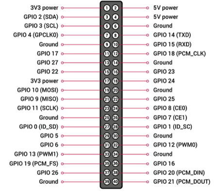
[10-FEB-25] We propose to replace the RCM6700 deployed in the A3050 with a RPi 3B+, like the ones we use in the A3034C. When we try to use the GPIO lines directly as a parallel interface, we immediately encounter three problems. First, any time we generate a rising edge on a GPIO, we see a 100-ns HI pulse, 500-ns LO, and then the rising edge we want. Second, we cannot write to more than one GPIO at a time. Third, when we toggle a single GPIO as fast as we can, it goes at only 100 Hz.
raspi-gpio set 2 op dl
raspi-gpio set 2 op dh
There are two SPI interfaces on the GPIO connector. We enable one on a 3B+ and see it trying to run at 100 MHz. We are trying to figure out how to set the speed from the command line, or the /boot/config.txt file. We come across the pigs utility. This utility is installed on our 3B+.
[11-FEB-25] We consult the RPi 40-Pin GPIO pinout, and the pinouts for RPi listed in the pigs manual, which we reproduce below.
                      MISO   MOSI   SCLK   CE0   CE1   CE2
           Main SPI      9     10     11     8     7     -
           Aux SPI      19     20     21    18    17    16
Here we have Master In Slave Out (MISO), Master Out Slave In (MOSI), Serial Clock (SCLK), and Chip Enable (CE). We can configure the SPI bus to have MISO default HI, and the CE lines can be positive-true or negative-true. We use the following lines to close any pre-existing Main SPI interface and send a single byte to MISO.
$ sudo pigpiod                                                   # Start pigs daemon.
$ ps -e | grep pigpiod
 7247 ?        00:00:02 pigpiod
$ pigs spic 0                                                    # Close handle zero.
-25
ERROR: unknown handle
$ pigs spio 0 1000000 0                                          # Open Main SPI at 1MHz.
0                                                                # The handle is 0.
$ pigs spiw 0 0xAA                                               # Transmits 1 byte.
$ pigs spiw 0 0xAA 0xAA 0xAA 0xAA 0xFF 0x00 0xFF 0x00 0x33 0x33  # Transmits 10 bytes.
$ pigs spic 0                                                    # Close handle zero.
$ pigs spiw 0 0xAA                                               # Write to handle zero.
-25
ERROR: unknown handle
We make sure the pigs daemon is running. We close any preexisting connection to the Main SPI, which is SPI number zero. We open a new connection to SPI zero, setting the SPI clock rate to 1 MHz and using default flags. We hook our oscilloscope up to SCLK, MOSI, and CE0.
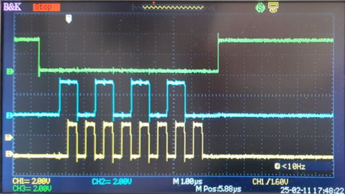
We increase the clock frequency to 20 MHz and try again. The clock frequency we observe is indeed 20 MHz. The signals show noise, but no significant overshoot. We see that the chip select line goes low 700 ns before the byte transmission.
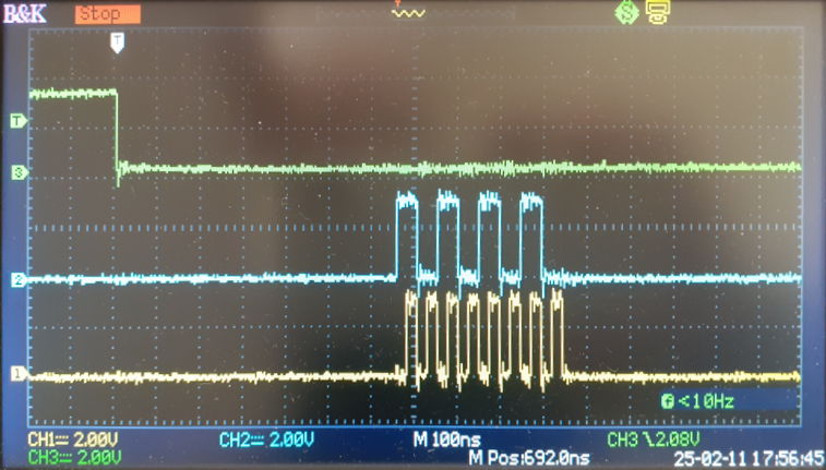
We transmit ten bytes and the entire transmission takes 6.5 μs, allowing for the delay after CS asserted and another 1 μs after CS unasserted. We transmit 40 bytes in 18 μs. It looks like we can achieve 2 MByte/s with this interface.
[17-FEB-25] We power up an RPi 3B+ from 5V through an ammeter. Current consumption during the first minute is 50-470 mA with a median of around 250 mA. After boot, we see 230-270 mA when the RPi is idle.
[18-MAR-25] We start the detailed design of this new PoE function generator with LWDAQ server. We will mount a Raspberry Pi 3B+ onto the board and connect to it using a short 40-way ribbon cable and a short 4-way ribbon cable, in the same way we do in our A3034C circuit.
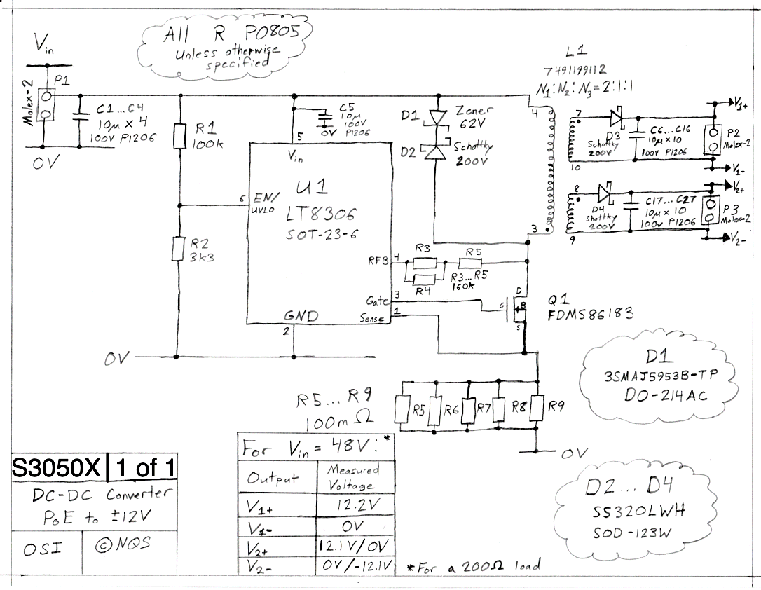
[19-MAR-25] We examine our existing S3050X converter design. We have been running the 5-V version for the past six months with a 5-Ω load. We just turned it off and put it away. The design uses the LT8306 no-opto flyback regulator. But there are a few problems we see with the design. The peak current in the switch is 10 A, but the transformer primary saturates at 1.3 A. There is no snubber ciruit to damp the ringing of the transformer, and we would like to minimize noise in our function generator. The circuit is complicated by an external switch, when we could be using the LT8304 regulator with internal switch. The transformer is too tall to fit in a standard module. We could be using something smaller and higher-current from Coilcraft.
We consider what is available in surface-mount, commercial off-the-shelf isolating DC-DC converters. We have been using the CC-E 48-V converters for five years with no failures. The dual-output versions are more difficult to find. We propose to use single-output only. We need to supply the RPi with up to 2.5 W, and we propose to obtain most of our 3.3-V power from the RPi's on-board converter. We suggest the CC6-4805SR-E, 6-W, 5-V output, $15 in QTY 50. For our function generator power amplifiers, we suggest two of the CC3-4812SR-E, 3-W, 12-V output, $10 in QTY 50. Our total converter cost is $35. With two 3-W, 12-V converters we can supply 250 mA from ±12 V. If we terminate two 10-V outputs with 50 Ω, we will draw 200 mA maximum. If we short one output and leave the other open circuit, we will draw up to 200 mA. If we short both outputs, the converter will shut down.
We look at converters in SIP-8 packages, 0.1" pitch, with between 5 and 7 pins loaded. We search for 3-W, 48-V input, single 12-V output and find 35 in stock at DigiKey, including RS3-4812S, MD348S-12CRW, AM3G-4812SEZ, SPBW03G-12, all with the same pinout. Dual-output converters in the SIP-8 also have a standard pinout. These converters are buit on their own circuit board with pins on one side, encapsulated in epoxy. The Traco Power TMR 12-4822WI is a 12-W, 48-V input, ±12-V output converter with a couple of extra case mounting pins, which we could cut off, and comes in a metal can, but otherwise standard pinout. The Cincon EC4SAW-48D12HN is a 6-W, 48-V input, ±12-V output converter for $14. Both claim >85% efficiency. The MeanWell SPBW06G-05 is a 6-W, 48-V input, 5-V output converter for $11. We resolve to place two SIP-8 converters on our board with P1206, 10-μF, 100-V input capacitors, and 10-μH, P0805, EMI blocking inductor.
[21-MAR-25] The original A3031 and subsequent A3050 function generators used the LT1206 ($11) high-current op-amp for both amplification and final power output. We propose to use one LM6172 ($3) dual op-amp for amplification and one LMH6321 ($3) for buffering. The first op-amp will take 0-3.0 V and turn it into ±5 V. The variable filter comes next, then another op-amp to turn ±5 V into ±10 V. Now comes the variable attenuator, and after the attenuator is the buffer and a2.4-W, 50-Ω output resistor, like the RCP1206W50R0GEB. The original circuits used the DG411DY analog switches to select resistors and capacitors for the filters and attenuators. These have channel resistance 25 Ω and channel-on capacitance 35 pF. Together, these give us a time constant of 0.9 ns, which is far less than the target 50-ns rise time of our new generator. Vishay Siliconix no longer makes the DG411DY, but other companies do. We will switch to the DG412DY, in which the switches close with a logic HI rather than a logic LO.
We will derive our main logic power from the RPi's converter, but we will derive the DAC digital output power supply from our own 5V0 using one TLV71330 3.0-V 1%-accurate regulator for each DAC. Our DAC output will be 0.0-3.0 V instead of the previous 0.0-3.3 V. We will route the eight DAC outputs of each channel through its own dedicated I/O bank on the logic chip. For our incoming PoE power switch, we will re-use the A3034C power receiver.
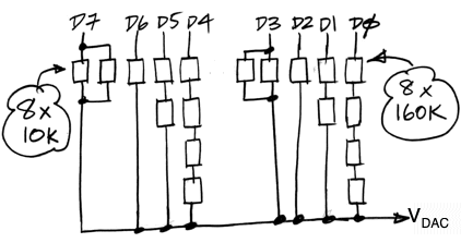
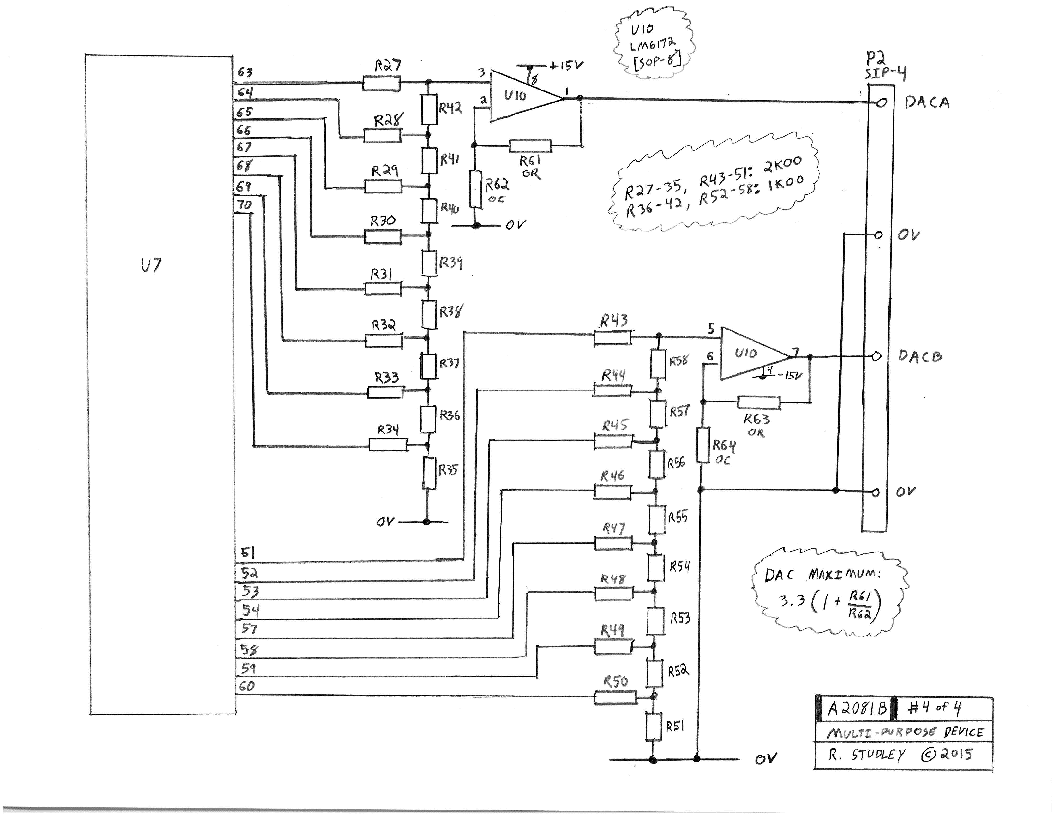
In the earlier circuits, we used two resistor values in parallel and series combinations to allow us to obtain precise factors of two from one bit to the next. We call this the eighteen-resistor DAC. We could try 0.1% resistors in values 10, 20, 40.2, 80.6, 160, 316, 642, and 1200 kΩ. We will have a 0.5% error in the third resistor, which is 0.1% of full range, or one quarter of a full step. Or we could use 4.87, 9.76, 19.6, 39.2, 78.7, 158, 316, 634 kΩ. This is the eight-resistor DAC. Another option is the sixteen-resistor ladder, as demonstrated by Richard Studley in his A2081 circuit. We have sixteen resistors of two values. We could use 10 kΩ and 20 kΩ. Output resistance is 10 kΩ. The two-value DAC circuits are cheaper to build, because they reduce the number of reels the assembly house must load onto their machine. The sixteen-resistor ladder requires that each output be able to drive a load of 3 kΩ or so. If we are going to increase current drive to the network, we must increase curren driver on all eight bits. But the eighteen-resistor network requires peak current only from the top bit, allowing us to provide 24 mA drive for the top bit, 8 mA for the second bit, and 4 mA for the rest. We will stick with the eighteen-resistor DAC.
[23-MAR-25] Our DAC output will have 256 states spanning 0.0-3.0 V. We use one half of an LM6172 to shift and amplity the DAC output so it spans ±5 V. We use the circuit shown below.
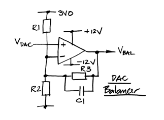
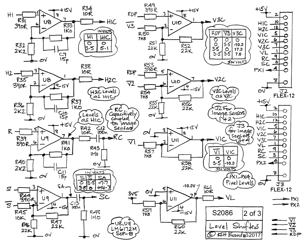
For the derivation that allows us to choose values for R1, R2, and R3, see DAC_Balancer_Eq. Example values that give a perfect result are R1 = 1.0 kΩ, R2 = 2.5 kΩ, and R3 = 1.7 kΩ. Other combinations are given in our DAC_Balancer_R table. Standard 1% values we can use are R1 = 1.00 kΩ, R2 = 2.49 kΩ, and R3 = 1.69 kΩ. We might add C1 = 15 pF to remove overshoot, as we do in the S2086 level-shifters.
The output from the DAC Balancer passes through the variable filter. The variable filter uses analog switches, let us assume they are DG412DY with 9-pF off capacitance and 35-pF on capacitance. Both these act as capacitance to ground from the drain or source or channel when the switch is off (open) or on (closed). To minimize the effects of these capacitances, we drive the resistor switches directly with our DAC Balancer, and we connect the capacitor switches directly to 0V.
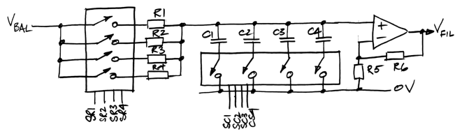
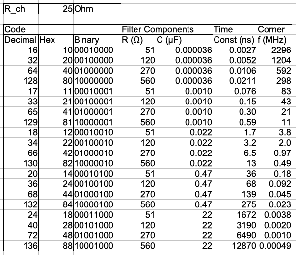
We must add to the resistor values the 25-Ω channel resistance of the switches. Following the pattern we used in the A3050, but accounting for the 25 Ω, and using standard values, we like R1 = 51 Ω, R2 = 120 Ω, R3 = 270 Ω, and R4 = 560 Ω. For the capacitors, we can try C1 = 1.0 nF, C2 = 22 nF, C3 = 470 nF, and C4 = 22 μF. These values produce the following time constants and corner frequencies.
[24-MAR-25] We devise a new variable attenuator circuit, consisting of a ladder of resistors. We have the analog switches connecting directly to ground. Let us assume the DG412DY as our switch. The on-state channel capacitance of 35 pF is charged and discharged by their on-state channel resistance of 25 Ω when the shunt resistor is connected to ground. Their off-state drain capacitance of 9 pF will be charged by the shunt resistors. Rise-time from these capacitances combined should be no more than 10 ns.
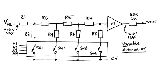
With the help of a Toolmaker script, we select suitable values of the shunt resistors. We fix the series resistors at 470 Ω and vary the others from 45 Ω to 1000 Ω in a brute force search for the shunt values that give us the most even progression of logarithmic attenuation.
These networks present a load of around 1 kΩ for most steps, but reaching a minimum of 800 Ω for the highest attenuation. Our LM6172 op-amp can drive ±10 V into 1 kΩ from a ±12 V power supply. In implementing the network, we will choose resistor values that, when added to the 25-Ω on channel resistance of the DG412DY shunt switches, will give a close match to our ideal values. The result is a network that provides sixteen steps of roughly 4 dB each, so that we have attenuation 0 dB to 50 dB. The resistors that give the orange plot are R1 = R3 = R5 = R7 = 470 Ω, R1 = 560 Ω, R4 = 390 Ω, R6 = 180 Ω, and R8 = 22 Ω. The expected values for the attenuation are given in the table below.
[29-MAR-25] Finish all four pages of the A3052AV1 schematic.
[25-JUL-25] We are now thinking we will use a two-part folded sheet metal enclosure for the A3052. Our existing enclosure needs to be re-designed, but we use the solid model to obtain a quote of $60 each in quantity 100. We are thinking of using the Raspberry Compute Module CM4002016 instead of the Raspberry Pi 3B+. For this, we must replace P1 with an RJ-45 socket, we must add a Ethernet physical layer chip, and we must replace P2 with two 100-way, 2-row SMT connectors. We must add an external SD card socket. We want to add one more general-purpose trigger input-output, and for this we need to add one more BNC-RA.
| Part | Cost ($) |
|---|---|
| Folded sheet metal enclosure | 60 |
| Raspberry Pi CM4002016 | 46 |
| DC-DC ±12V 9W, DPB09C-12 | 13 |
| DC-DC +5V 6W, SPBW06G05 | 13 |
| FPGA, LCMXO2-4000HC | 20 |
| Ethernet PHY, KSZ9031 | 2 |
| Analog Switches, 6×DG412DYZ | 9 |
| Amplifiers, 4×LM6172IMX | 12 |
| Buffers, 2×LMH6321MRX | 6 |
| Connectors, 4×BNC-RA | 24 |
| PCB, A305201A, PCBWay | 10 |
| Assembly, A3052AV1, PCBWay | 11 |
| Connectors, 2×DF40C-100DS-0.4v | 2 |
| Connector, 1×7499210121A | 7 |
| Resistors, inductors, capacitors | 10 |
| Transistors, chips, LEDs | 10 |
| Spacers, screws, light pipes | 10 |
| Total | 265 |
The CM4 version ends up being more expensive because of the physical layer chip and the RJ-45 connector, which together add $10 to the cost with assembly, and then the CM4 is $8 more expensive than the Raspberry Pi 3B+. But the RPi 3B+ requires a short 40-way ribbon cable, a short 4-way ribbon cable, and both 40-way and 4-way SMT headers. The parts for these cost around $5 total and they require assembly.
| Part | Cost ($) |
|---|---|
| Folded sheet metal enclosure | 60 |
| Raspberry Pi 3B+ | 37 |
| DC-DC ±12V 9W, DPB09C-12 | 13 |
| DC-DC +5V 6W, SPBW06G05 | 13 |
| FPGA, LCMXO2-4000HC | 20 |
| Analog Switches, 6×DG412DYZ | 9 |
| Amplifiers, 4×LM6172IMX | 12 |
| Buffers, 2×LMH6321MRX | 6 |
| Connectors, 4×BNC-RA | 24 |
| PCB, A305201A, PCBWay | 10 |
| Assembly, A3052AV1, PCBWay | 10 |
| Ribbon cable and IDC connectors | 3 |
| Resistors, inductors, capacitors | 10 |
| Transistors, chips, LEDs | 10 |
| Spacers, screws, light pipes | 10 |
| Total | 247 |
The cost difference is not great, but the RPi 3B+ boots off an SD card, and is the same platform we are familiar with in the A3034C. With suitable apertures on the back wall of the enclosure, the user will have access to four USB ports. Another possibility is to provide access to spare GPIO lines with a DB-25 socket on the back wall. If we add a couple of eight-bit ADCs for the trigger inputs, we can provide digitization synchronous with the function generator output. The RPi 3B+ will be in production until at least January 2028. We consider the RPi 4, which will be in production until 2034. It is $20 more expensive. According to user reports, the RPi 4 consumes around 3 W quiescent, which is twice what we observe for the RPi 3B+. Our total power budget for the A3052 is 10 W. We have maximum power to function generator outputs 2 * 2 W = 4 W. Roughly 3 W for other analog and digital circuits, and 3 W for the RPi is 10 W. So we could use the RPi 4. Both versions have identical profiles, hole locations, and header locations. But their Ethernet and USB sockets are swapped around. We discuss how the back wall will look and decide we can have a single rectangle for all three connectors, so it won't matter if they swap places.
[29-JUL-25] We would like whatever TCP/IP solution we come up with for the A3052 to serve also on our long-term upgrades to the ALT, TCB, and LWDAQ Driver. We would like it to serve on our new Detector Module Test Fixture (A3038DMTF). But we now consider a potential problem with any Linux system when implementing a LWDAQ Relay. There is a "byte poll" job that the LWDAQ Controller needs to execute and be followed immediately by image readout during BCAM acquisition. The image readout must not be delayed with respect to the byte poll by more than a millisecond, and whatever the separation is, it must be constant. If the delay varies, the background intensity in our BCAM images will vary. Linux does not provide real-time response from any one process. It is a pre-emptive multi-tasking operating system. The polling of a byte in the LWDAQ Controller by a Linux LWDAQ Relay could be interrupted, and if it is interrupted, we will have to wait. According to ChatGPT, interrupt latency on the RPi is typically less than 100 μs but can be as great as 2 ms. This latency will undermine our readout of radiation-damaged image sensors. The byte poll cannot be performed by a Linux process.
The RPi SPI interfaces cannot be configured as slaves. The SPI interface is master-slave and synchronous, while the TCP/IP interface is client-server and asynchronous. The RPi does provide UARTS (Universal Asynchronous Receiver-Transmitters), but their absolute top recorded speed is 4 Mbps, which would be no more than 500 kByte/s. We want at least 2 MByte/s to transfer images from a LWDAQ controller memory to the LWDAQ Relay. So the UARTS are not fast enough. If we forward the LWDAQ messages through the RPi to an OSR8 processor running in our controller logic, the OSR8 can perform byte polls and writes, but as soon as we want to read from the controller, we have a problem with the SPI interface: how is the RPi process going to know when to read the data from the OSR8. ChatGPT calls this a "classic architectural impedance mismatch", and goes on to say "You're trying to bridge an asynchronous, peer-to-peer protocol (Ethernet/TCP/IP) with a synchronous, master-slave protocol (SPI), and that friction becomes acute with stream reads initiated from the peripheral side."
We suggest the following scheme. In the controller logic, which will be a MachXO2 chip with at least one OSR8 processor running on it, one dedicated to handling communication with the RPi. We provide a buffer for the SPI interface. We invert the buffer empty flag and use it to drive Byte Ready (BRDY) using a GPIO line on the RPi. We use another GPIO line as "READ", which the RPi delivers to the controller. When the RPi asserts READ and transmits a byte on the SPI interface, the controller reads the byte and adds it to its input buffer. When the RPi unasserts READ and transmits a dummy byte on the SPI interface, the controller transmits a byte from its buffer. We assume that the RPi will read only when BRDY is asserted. By this means, we permit the controller to initiate byte transfers. The RPi takes the bytes it reads and transfers them immediately to the TCP/IP socket. We discuss this with ChatGPT, and it approves.
We now consider whether we can get rid of the controller RAM present on all existing controllers. The A2071E, for example, has 8 MByte of 10-ns static RAM. The RPi has a Gigabyte of LPDDR2 SDRAM. As we read bytes from an image sensor, can we transfer them directly to the RPi memory? Right now, we can read and write to random locations in the controller memory using the data address register. The controller can also digitize pixels returned from an image sensor at a constant 2 MPS and store them immediately in memory. We have a second SPI interface our controller can use to communicate with the RPi. Let us assume that the RPi can read bytes out of this interface at a sustained 2 MBPS, but that the readout process might be interrupted for 3 ms. We would need to store 6000 bytes in a buffer on the controller side. Our LCMXO2-7000HC has 26 KByte of RAM. On the A3052, we need 8 KByte for each waveform. On a LWDAQ driver we could dedicate much of this to a buffer, but a 10-ms latency would cause an overflow, and a 10-ms latency is possible. We can, however, solve this buffering problem with a 512-KByte SRAM on the controller. This could act as a FIFO for the SPI interface. But we still need to specify where in the RPi-resident controller memory space we want bytes to go, and we still need to be able to read bytes out of this memory using the controller.
[30-JUL-25] Checking the value of BRDY before reading may also be a problem. The time it takes to read a GPIO could be prohibitively long. When we wrote to a GPIO earlier, we were not able to get it to go faster than 100 Hz. Further investigation with ChatGPT reaveals that if we set up direct memory mapping of the GPIO space into our user memory, we can read and write to GPIOs in 50 ns, and furthermore we can set and clear them in 32-bit clusters. The chatbot provides the following code for a library that provides initialization of the memory mapping and implementation of a write function.
library gpiobus;

uses
  baseunix, unix, sysutils;

const
  BCM2837_PERI_BASE = $3F000000;
  GPIO_BASE         = BCM2837_PERI_BASE + $200000;
  BLOCK_SIZE        = 4096;

var
  gpio_map  : pointer = nil;
  gpio      : PLongWord = nil;
  mem_fd    : cint = -1;

function init_gpio: cint; cdecl;
begin
  if gpio <> nil then begin
    init_gpio := 0;  // Already initialized
    Exit;
  end;

  mem_fd := fpopen('/dev/mem', O_RDWR or O_SYNC);
  if mem_fd < 0 then begin
    init_gpio := -1;
    Exit;
  end;

  gpio_map := fpmmap(nil, BLOCK_SIZE, PROT_READ or PROT_WRITE, MAP_SHARED, mem_fd, GPIO_BASE);
  if gpio_map = MAP_FAILED then begin
    init_gpio := -2;
    Exit;
  end;

  gpio := PLongWord(gpio_map);
  init_gpio := 0;
end;

procedure write_bus_byte(addr, data: byte); cdecl;
const
  DATA_SHIFT   = 10;
  ADDR_SHIFT   = 18;
  WR_MASK      = 1 shl 24;
  STROBE_MASK  = 1 shl 25;
  BUS_MASK     = ($FF shl DATA_SHIFT) or ($3F shl ADDR_SHIFT) or WR_MASK;
var
  value: LongWord;
begin
  if gpio = nil then
    if init_gpio <> 0 then
      Exit;

  value := (LongWord(data) shl DATA_SHIFT) or
           (LongWord(addr) shl ADDR_SHIFT) or WR_MASK;

  gpio[10] := BUS_MASK;   // Clear bus
  gpio[7]  := value;      // Set data/address/write
  gpio[7]  := STROBE_MASK;

  // Delay ~50–100 ns
  asm
    nop
    nop
    nop
    nop
  end;

  gpio[10] := STROBE_MASK or BUS_MASK;
end;

exports
  write_bus_byte,
  init_gpio;

begin
end.
Another way to build a LWDAQ Relay is with a PIC32MZ2048EFH100 microcontroller and LAN8720A Ethernet physical layer. The PIC32MZ will run at 200 MHz and it includes a Media Access Controller (MAC). It provides a reduced media-independent interface (RMII) to communicate with the physical layer. A C-complier and programmer with graphical user interface runs on MacOS, Linux, and Windows. We have installed the program and it runs without error. The microcontroller provides an external bus interface that we can use to interact with external logic, such as the A3052's function generator logic or a LWDAQ Controller's logic. We could in principle put these chips on an mPCIe board and so produce a replacement for the RCM6700. The TCP/IP stack is provided for free by Microchip Technology, and includes support for the LAN8720A. If we were to build an RCM6700 replacement in this way, we would now have a 32-Bit MCU running at 200 MHz. We would have complete control over all timing and ports.
| Part | Cost ($) |
|---|---|
| PIC32MZ2048EFH100 | 14 |
| LAN8720A | 1 |
| ABM8G-25.000MHZ | 1 |
| mPCIe PCB | 10 |
| Regulators | 2 |
| Miscellaneous | 2 |
| Assembly | 10 |
| Total | 40 |
Suppose we build such a board. We don't have to re-design our ALT, TCB, nor even our POEFG because we already have the RCM6700 design worked out. We can use our existing A2071E design and firmware. We work on getting the LWDAQ Messaging exactly right and debuggedl and then we are going to be done working on this for another ten years. Meanwhile, we can provice embedded microprocessor designs for consulting contracts that use this same MCU and development system. We have one such consulting job in mind.
[23-MAR-26] We are going to use the A3053 Embedded Ethernet Module to provide our network interface. We re-draw page two of the S3052 schematic to accommodate the A3053, deleting the previous Pi-based design. Now we will have both Telnet and LWDAQ interfaces, with a nice command-line interface in the Telnet server to provide all the control we need over the A3052.
[27-MAR-26] Complete updated Page Two of the S3052 schematic. Choose signals to route directly from a twenty-five way D-sub socket on the back of the A3052 to the PIC32MZ on its A3053 Embedded Ethernet Module.