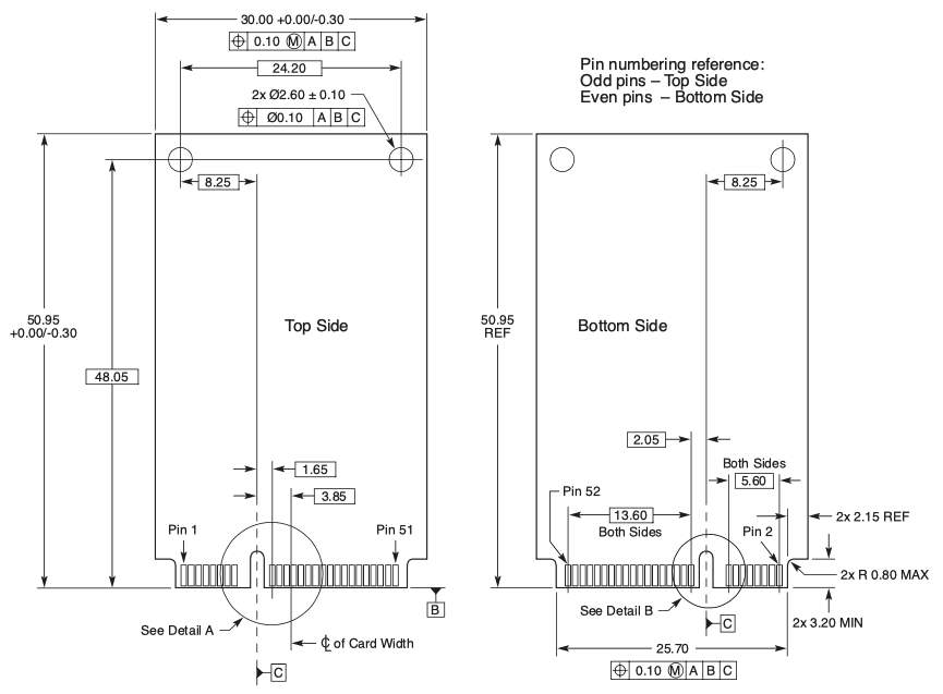
| Description |
| Pin Assignments |
| Source Code |
| Programming |
| Persistent Configuration |
| Command-Line Interpreter |
| Indicator Lamps |
| Test Points |
| RCM6700 Compatibility |
| Licensing and Copyright |
| Design |
[01-JUL-26] The A3053 provides a wired network connection and a fast logic interface for a scientific instrument, an industrial process controllers, or a piece of test equipment. The A3053 is built on an industry-standard mPCIe card. It mounts upon one of the electronic circuit boards board in its host instrument and communicates with the host board logic through its mPCIe pins and with the local area network through an RJ-45 socket provided by the host board. The A3053 built on an mPCIe card, powered by a PIC32MZ2048EFH microcontroller, and provides a versatile, high-speed logic interface for communication with its host. Examples of instruments in which we deploy the A3053 are the A3042 Telemetry Control Box (TCB), the A3038 Animal Location Tracker (ALT), the A2071E LWDAQ Driver with Ethernet Interface, and the A2087 TCPIP-VME Interface. In each of these instruments, the host board provides an mPCIe socket for the A3053 to sit in, and an RJ-45 socket for the network connection. The A3053 provides forty programmable connections between microcontroller and its mPCIe connector. You can use these connecctions in any way you like. You can use them to implement a sixteen-bit parallel interface with 50-ns access time, or you can use them to create multiple 20-Mbps synchronous serial ports. If you add a Power-over-Ethernet (PoE) converter to your instrument, you can provide both power and communication with a single cable connected to a PoE switch. Because communication with the A3053 takes place over TCP/IP, you have no need of special software drivers for different computer operating systems. When you program the A3053 with our free, open-source P3053 software, you can use Telnet to connect to the module immediately and interact with a built-in command line interface.
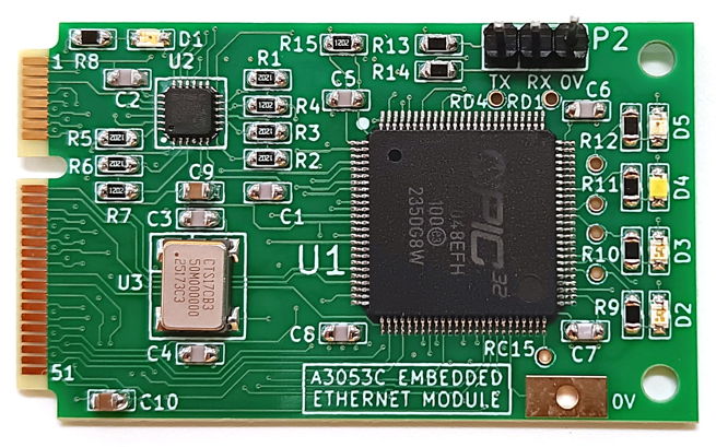
The heart of the A3053 Embedded Ethernet Module is a PIC32MZ2048EFH "Embedded Connectivity with Floating Point Unit MCU" in a TQFP-100 package. This particular variant of the PIC32MZ family is equipped with 2 MByte of flash memory and 512 KByte of random-access memory (RAM). The PIC32MZ microcontrollers use the MIPS32 M4K instruction set. The A3053 runs its PIC32MZ at 200 MHz. The TQFP-100 package provides fifty-one general-purpose input-output (GPIO) pins, of which forty are routed by the A3053 to pins on the mPCIe connector. These pin include 12-bit analog-to-digital converter (ADC) inputs, pulse-width modulated (PWM) outputs, and tri-state buffers. The PIC32MZ provides its own media access controller (MAC), but not an Ethernet physical layer. The A3053's Ethernet physical layer is provided by a LAN8720A. Also mounted on the A3053 are a 50-MHz oscillator, five LEDs, and a collection of capacitors and resistors. There are no parts on the underside of the board.
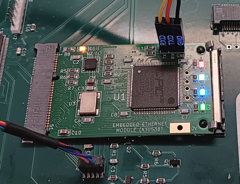
The A3053 Embedded Ethernet Module provides a three-wire UART serial console that we can use to communicate directly with its microcontroller. We load 3×1 header into footprint P2 on the A3053 circuit board and connect it to a USB-to-UART bridge. When we program the A3053 with the P3053 demonstration software, this serial interface provides a Command-Line Interpreter (CLI) through which we can query and control the A3053 without passing through the host board or network socket. Once the A3053's network interface is up and running, however, we can communicate with the same CLI over the network by connecting to the A3053's Telnet server.
We designed the A3053 Embedded Ethernet Module to take the place of the discontinued RCM6700 Ethernet module in our own network-enabled data acquisition circuits. The RCM6700 was discontinued by its manufacturer in December 2024. The A3053 is a general-purpose, reconfigurable mPCIe Ethernet module in the same mPCIe format as the RCM6700, and has been performing well in place of the RCM6700 in our circuits since December 2025. If you are looking for an Ethernet module to take the place of the RCM6700, there is a good chance that the A3053 will be able to satisfy your requirements. We hope that the information and links provided by our RCM6700 Compatibility and Design chapters will permit you to determine for certain whether or not you can program the A3053 to act as a replacement for the RCM6700 on your own instrument. Although the A3053 is an open-source design, we fully support and encourage users of the A3053 to equip the module with their own proprietary software. See the Software Licenses chapter below for details of the A3053's copyright restrictions and how to break free of them to produce your own private source code.
We program the A3053 Embedded Ethernet Module through a plug on the host board. We use a Microchip PICKit 5 programming cable, which we connect with a USB cable to the same computer upon which we are editing and compiling our branch of the P3053 software. The PICKit supports a variety of programming plugs. A 6×1 0.1" SIP header is a typical choice for Microchip devices. If we are loading an A3053 onto a host board that was designed for the discontinued RCM6700 module, there will be a 5×2 0.05" header on the host board for programming an RCM6700. We can use this same header to program the A3053. See the Programming chapter below for more details.
[26-MAR-26] The table below gives the connections between the components on the A3053C Embedded Ethernet Modules and its mPCIe connector pads. For all signals, we give the P1 mPCIe pin number. For signals connected to the U1 PIC32MZ, we give the U1 pin number. For signals connected to U2 LAN8720A, we give the U2 pin number. For each mPCIe pin, we give a full list of the PIC32MZ functions the pin makes available to the host board. If the pin is reserved for a particular A3053 function, we name that function. Functions with names "ANx", where x is a number, are twelve-bit analog to digital converter (12-bit ADC) inputs. The pair "SCL2" and "SDA2" form an I2C bus. For details of the many functions provided, see the PIC32MZ data sheet.
| mPCIe Pin | A3053C Signal |
|---|---|
| P1-1 | 0V |
| P1-2 | 3V3 |
| P1-3 | U2-21, TXP |
| P1-4 | U2-23, RXP |
| P1-5 | U2-20, TXN |
| P1-6 | U2-22, RXN |
| P1-7 | U2-3, LINK |
| P1-8 | 3V3, ECOM |
| P1-9 | U1-97, TRD0/SQID0/RG13 |
| P1-10 | U1-96, TRD1/SQID1/RG12 |
| P1-11 | U1-10, AN14/C1IND/ECOL/RPG6/SCK2/RG6 |
| P1-12 | U1-28, VREF-/CVREF-/AN27/AERXD2/RA9 |
| P1-13 | U1-11, EBIA4/AN13/C1INC/ECRS/RPG7/SDA4/PMA4/RG7 |
| P1-14 | U1-29, VREF+/CVREF+/AN28/AERXD3/RA10 |
| P1-15 | U1-23, AN2/C2INB/RPB2/RB2 |
| P1-16 | U1-15, !MCLR |
| P1-17 | U1-20, AN45/C1INA/RPB5/RB5 |
| P1-18 | U1-4, EBID6/AN16/PMD6/RE6 |
| P1-19 | U1-22, AN3/C2INA/RPB3/RB3 |
| P1-20 | U1-5, EBID7/AN15/PMD7/RE7 |
| P1-21 | U1-26, PGEC2/AN46/RPB6/RB6 |
| P1-22 | U1-27, PGED2/AN47/RPB7/RB7 |
| P1-23 | U1-32, EBIA10/AN48/RPB8/PMA10/RB8 |
| P1-24 | U1-33, EBIA7/AN49/RPB9/PMA7/RB9 |
| P1-25 | U1-34, EBIA13/CVREFOUT/AN5/RPB10/PMA13/RB10 |
| P1-26 | U1-43, EBIA1/AN9/ERXD2/AETXD3/RPB14/SCK3/PMA1/RB14 |
| P1-27 | U1-44, EBIA0/AN10/ERXD3/AETXD2/RPB15/OCFB/PMA0/RB15 |
| P1-28 | U1-1, !RST |
| P1-29 | U1-91, EBID0/PMD0/RE0 |
| P1-30 | U1-94, EBID1/PMD1/RE1 |
| P1-31 | U1-98, EBID2/PMD2/RE2 |
| P1-32 | U1-99, EBID3/RPE3/PMD3/RE3 |
| P1-33 | U1-100, EBID4/AN18/PMD4/RE4 |
| P1-34 | U1-3, EBID5/AN17/RPE5/PMD5/RE5 |
| P1-35 | U1-17, TMS/EBIA16/AN24/RA0 |
| P1-36 | U1-38, TCK/EBIA19/AN29/RA1 |
| P1-37 | U1-59, EBICS0/SCL2/RA2 |
| P1-38 | U1-60, EBIRDY1/SDA2/RA3 |
| P1-39 | U1-61, EBIA14/PMCS1/PMA14/RA4 |
| P1-40 | U1-2, EBIA5/AN34/PMA5/RA5 |
| P1-41 | U1-89, TRCLK/SQICLK/RA6 |
| P1-42 | U1-90, TRD3/SQID3/RA7 |
| P1-43 | U1-6, EBIA6/AN22/RPC1/PMA6/RC1 |
| P1-44 | U1-24, PGEC1 |
| P1-45 | U1-7, EBIA12/AN21/RPC2/PMA12/RC2 |
| P1-46 | U1-8, EBIWE/AN20/RPC3/PMWR/RC3 |
| P1-47 | U1-25, PGED1 |
| P1-48 | U1-9, EBIOE/AN19/RPC4/PMRD/RC4 |
| P1-49 | U1-21, AN4/C1INB/RB4 |
| P1-50 | U1-40, TDO/EBIA17/AN31/RPF12/RF12 |
| P1-51 | 0V |
| P1-52 | +3V3 |
In the A3053C Embedded Ethernet Module mPCIe Pinout table, we name the PIC32MZ connections after the shortest and simplest name assigned to them in the PIC32MZ data sheet Table 3. When the connection is reserved for a particular PIC32MZ function, we give the name of that funcion as well. The !MCLR signal must be a global negative-true reset signal provided by the host board. It must be asserted for at least 10 ms once the power supplies have settled. It must be debounced by a host board reset monitor if there is a host board reset switch. When !MCLR is asserted, the PIC32MZ resets immediately. The !RST signal is generated by the A3053 when it boots up, and is asserted for at least 10 ms. The A3053 uses !RST to reset its Ethernet physical interface. The host board can make use of !RST in any way it sees fit. The A3053 pulls up !RST with a 12-kΩ resistor and drives the signal LO when it wants to assert !RST, but never drives the signal HI. The host board can likewise assert !RST, but must not drive it HI. When the host board asserts !RST, the Ethernet physical interface will reset but the PIC32MZ will not. The Ethernet connections on the mPCIe card edge are TXP, TXN, RXP, RXN, and ECOM. The ECOM signal is the Ethernet common-mode voltage, which the A3053 connects to the 3V3 power supply, which is nominally 3.3 V supplied by the host board. The PGEC1 and PGED1 signals are the ones we use to program the A3053's PIC32MZ microcontroller. The host board must provide a connector for a PIC progamming cable to plug into. See the Programming chapter for programming details.
[13-MAR-26] To enable rapid deployment of the A3053 Embedded Ethernet Module on new host boards, we provide a repository of code that will immediately enable you to communicate with the A3053 once you load it into your host board. Our P3053 GitHub repository contains all the source code that defines our embedded TCP/IP server with mPCIe parallel interface. To complete the compilation and linking of the PIC32 executable, you also need the PIC32MZ2048EFH device package and linker script, which you can download from our website as PIC32MZ-EF_DFP.zip. Unpack this archive and you will have a directory named PIC32MZ-EF_DFP. We place the PIC32MZ-EF_DF directory in a Microchip directory adjacent to our P3053 repository. If you do the same, you do not need to edit the makefile to point to your own device package. But if you put the package somewhere else, edit the following lines in the P3053 makefile so they point to your own location.
CPU := 32MZ2048EFH100
DFP_DIR := $(abspath ../Microchip/PIC32MZ-EF_DFP/1.3.58)
CPULD := $(DFP_DIR)/xc32/$(CPU)/p$(CPU).ld
To compile and link a P3053 executable file, we use Microchip's xc32 tool chain. Download the xc32 installer from Microchip's website. Install the compiler and linker on your laptop so that they will run from the command line. After installing xc32, edit the P3053 makefile so that MP_DIR points to the directory in which you installed the xc32 binaries. In our case we have our Microchip files in "/Applications/microchip/xc32/v4.60/bin". To manage the executable build, we use "GNU Make 3.81". Open a terminal, navigate to the P3053 directory, and type "make". This same procedure works on Windows, Linux, and MacOS, although on Windows you will first have to install a Linux shell such as Git-Shell. After typing "make", you will see the build progressing. If the build completes, you will find a hexadecimal file "P3053.hex" will appear in the "P3053/build" directory. This is the file we use to program the PIC32MZ. Our build system makes no use of the Microchip's "MPLAB X" graphical development environment. To edit files, we use a text editor, such as Sublime (Linux, MacOS, Windows), BBEdit (MacOS), or Crimson Editor (Windows). All of these editors allow us to collect source files together in a project folder for easy navigation and searching. All of them provide C-code hilting.
The code that manages the A3053 Embedded Ethernet Module's Ethernet physical interface, provides the TCP/IP stack, manages the UART interface, and sets up the interrupt timers resides in our "src/microchip" directory. These files are provided by Microchip and are taken from their Harmony3 libraries. The Harmony3 source code is free and provided with no license restrictions, although we must preserve their copyright notices. The code provided by Open Source Instruments (OSI) is in the "src" directory. This code is also free, but we issue it under the GNU Public License, which prohibits its inclusion in any code project that is not itself distributed for free under the same license. Our P3053 repository does not include the WolfSSL library that Microchip uses to provide Secure Socket Layer (SSL) services. Nor does it include Microchip's cryptography libraries. We eliminated both these libraries because we have no use for them and they were slowing down our build process. We can conceive of no application at OSI in which a data acquisition computer would need to serve an SSL to a client, nor any application where one of our instruments would be required to connect to an HTTPS server to upload data. Nor do we include in our P3053 repository the Harmony3 HTTP server library. We at first thought it would be useful to have an HTTP interface to configure the A3053, but when we came to actually working on the A3053, we found that the console and Telnet command-line interpreters were far more useful and versatile to us than any HTTP interface could be. With the Telnet server, we can turn on and off debug reporting, direct debug reporting to our telnet server, and re-write the A3053's non-volatile configuration. We can even use the Telnet interface to disable the Telnet server permanently until the user performs a factory reset of the module.
The OSI code consists of the files listed below. Each library consists of two files: an interface and an implementation. The interface file, or "header file", declares the shared functions provided by the library, and contains comments explaining in detail the purpose and proper usage of these functions. The implementation file, or "C file", defines the library functions and contains comments explaining in general terms how the functions work. We trust that the code itself will reveal how each function works in detail.
cli.c		console.c	main.c		server.c	utils.h
cli.h		console.h	microchip	server.h
config.c	lwdaq.c		pic.c		shim
config.h	lwdaq.h		pic.h		utils.c
As we provide it, the P3053 source code sets up two servers: Telnet and LWDAQ. Anyone can connect to the Telnet server with the "telnet" utility, the "nc" utility, or with a Python or Tcl socket channel. The Telnet server provides a command-line interpreter (CLI). Type "help" to get a list of available commands. Type "command --help" to get detailed help for a single command. The CLI's "mpcie" command allows us to read and write from the mPCIe parallel bus. This network access to the mPCIe bus is available as soon as we boot up the A3053 Embedded Ethernet Module. The Telnet server is designed for text-only communication. We have programmed it to ignore Telnet control characters. When we read bytes from the mPCIe bus, they will come back as text strings. The Telnet server's TCP socket is managed by our generic "tcpip_server" state machine. In the main.c file, we see the Telnet's server description record being composed and the Telnet server task function being defined. We see the task function composing a channel description record for each Telnet client socket and then using this record to provide the CLI to the client. In console.c, we set up the PIC32MZ's UART2 interface to act as the destination for operational and diagnostic reporting. In the "console_start" function, we see the connection being made between the console UART interface an our CLI. The console and its CLI allow us to obtain reports from the A3053, and query and modify its configuration, even without a working network connection.
Although useful during development and testing, the Telnet interface provided by the A3053 Embedded Ethernet Module is not fast enough to support real-time data acquisition in our own instruments. The fastest download we are able to get over the telnet interface is with the CLI's "mpcie stream-read addr len --packed" command. This command provides us with 5 kByte/s. We want fast, binary communication for data acquisition, and for that we use our own LWDAQ binary messaging protocol. The P3053's lwdaq.c file provides routines to receive and interpret LWDAQ messages, acknowledge them, and upload binary data to the client. When we start a TCP/IP server with "lwdaq_tasks" as its task function, the server will be a LWDAQ server. In lwdaq.c we see how the server achieves fast and reliable binary communication as well as rapid opening and closing of sockets without losing any data. We see how we can use the "tcp_tick" routine to maintain the TCP/IP stack and Ethernet interface while polling bytes on the host board with the mPCIe bus. The LWDAQ stream read moves data out of the host board RAM and uploads it to the client at about 2.1 MByte/s on a local wired network. The transfer from RAM is taking place at 3.6 MByte/s and the upload over TCP/IP is taking place at 5 MByte/s. With the LWDAQ server as an example, we hope new users of the A3053 will find it easy to prepare servers for their own binary TCP/IP data acquisition protocol.
The A3053 Embedded Ethernet Module's Telnet and LWDAQ servers service one socket at a time, but each provides its own socket queue so that multiple clients can use the server by taking turns. The turn-taking is not so useful for the Telnet server, in which clients tend to connect for a long time, but in the LWDAQ server, in which sockets open and close in a fraction of a second, the queue allows multiple clients to share the same server. By default, the queue contains four slots, and these do not include the active socket or the listening socket, so we can share the server between five clients without any timeout occurring. The queue is provided tcpip_server, along with a timeout counter for the active socket, so your protocol task server does not need to worry about the queue or keeping track of timeouts in its active socket. The queued sockets are not subject to a timeout until they become active.
[01-JUL-26] When we receive a new A3053 Embedded Ethernet Module, it will arrive with the PIC32MZ erased. When we plug it into our host board, the PIC32MZ will do nothing. The Ethernet PHY will connect to your switch, but the PIC32MZ will not start its TCP/IP stack. It will not start listening for connections. It will not start any kind of server. We must program the PIC32MZ to activate it. Once programmed with our default P3053B demonstration board software, the A3053 will be listening on port 23 for a Telnet connection and on port 90 for a binary LWDAQ connection. If we do not want our A3053 to provide a Telnet server, we must set EEM_TELNET_ENABLE flag to "false" in config.h. Likewise, if we do not want a LWDAQ server, we set EEM_LWDAQ_ENABLE to "false". We program the A3053 Embedded Ethernet Module's PIC32MZ microcontroller using the ICSP programming interface consisting of pins PGEC1, PGED1, and !MCLR. These signals appear on mPCIe pins P1-44, P1-47, and P1-16 respectively. We make these pins available for programming by means of a connector on the host board. One standard programming connecctor is a 2.54-mm pitch, 1×6 plug we call a SIP-6. Microchip defines a standard pinout for the SIP-6 programmer, as shown in our SIP-6 Programming Connections table.
| Pin | Signal | Notes |
|---|---|---|
| 1 | !MCLR | Microcontroller Clear, Negative True, P3053 mPCIe Pin 16 |
| 2 | VDD | Positive Power Supply, +3.3 V |
| 3 | GND | Negative Power Supply, 0.0 V |
| 4 | PGD | Programming Data, P3053 mPCIe Pin 47 |
| 5 | PGC | Programming Clock, P3053 mPCIe Pin 44 |
| 6 | NC | No Connection |
The ICSP programming interface uses two dedicated signals that pass through the mPCIe connector to the PIC32MZ. It also uses the global reset line, which is called !MCLR in the PIC32MZ data sheet. This line must be an open-drain signal that the ICSP programming cable can drive LO to cause a global reset, and then release to bring the system out of reset. The host board should provide a reset monitor that asserts !MCLR on power-up for 100 ms or so, and also debounces !MCLR when it is asserted with a push-button switch, but otherwise does not delay the release of !MCLR more than 10 ms after all other sources of !MCLR have released the line. Somewhere on the host board, !MCLR needs to be pulled up by a resistor.
[09-MAR-26] The configuration of the A3053 Embedded Ethernet Module is stored in flash memory, so it is persistent through power cycles and resets. We can restore the configuration to its factory default state by performing a configuration reset. An instrument equipped with an A3053 should provide a reset button and configuration button accessible from the outside of its enclosure. The reset button will assert the A3053 reset line, and the configuration button will clear the least significant bit of a location in the mPCIe parallel bus memory space. We use location 0x28 for this purpose (decimal 40), but the P3053 software can be modified to use any location. The A3053 checks the state of this bit after reset, and if the bit is cleared, it overwrites the flash configuration with the factory default configuration. The A3053 itself provides no reset or configuration switches. These must be provided by the host board. In the case of the configuration switch, pressing the switch clears bit zero in the configuration register location in the mPCIe address space. In our own P3053 implementation, we hold the configuration switch down for three seconds after releasing the reset button in order to accomplish a factory reset. By means of the configuration switch, we can restore the A3053 to a known state should we forget its IP address, or if its IP address is set to an inconvenient value. The factory reset configuration is like this:
static const eem_config_type eem_config_factory = {
	.flash_magic = CONFIG_FLASH_MAGIC,
	.seclevel = 0,
	.password = "LWDAQ",
	.person = "unassigned",
	.ip_str = "10.0.0.37",
	.gw_str = "10.0.0.1",
	.nm_str = "255.255.255.0",
	.timestamp = "00000000000000",
	.device = EEM_PLATFORM,
	.lwdaq_port = 90,
	.telnet_port = 23,
	.lwdaq_timeout = 10,
	.telnet_timeout = 300,
	.tcp_tick_ms = 2
};
Among the configuration parameters is a security level and password. These control access to the A3053 Embedded Ethernet Module and its configuration records. There are three configuration records available in the A3053: active, factory, and flash. The active configuration is the one that was read from flash memory on start-up. The flash configuration is the one currently residing in flash, which will be different from the active after we perform a modification. The factory configuration can be read but not modified. Nor can the active configuration be modified except when it is read from flash memory up after reset. If the security level is zero, no login is required to connect to and make full use of the A3053, including reading and modifying its configuration records. If the security level is one, we must provide the password in order to read any of the configuration records or modify the flash configuration record. If the security level is two, we must provide the password before the A3053 will allow us to perform any operation other than a password login operation. In our P3053 software, our Telnet and LWDAQ servers, as well as our UART serial interface, all respect the security level setting, although the serial interface behaves slightly differently. When the serial interface's command-line interpreter starts up, its logged-in flag is set. But for connections to the Telnet and LWDAQ servers, the logged-in flag is cleared until a successful login occurs.
The A3053 Embedded Ethernet Module's Telnet and LWDAQ servers listen on ports assigned by the two configuration port parameters. The LWDAQ server is the one we use for our data acquisition instruments, and in our P3053 code, the LWDAQ server provides an example of how to implement a binary messaging protocol for data acquisition. If we set either port to zero, the server will be disabled. The Telnet port provides a command-line interpreter, and we can use this to modify the A3053 flash configuration. Here is the help text provided by the interpreter's "config" command.
config --help
Usage:
  config [--info|--help]
  config show <active|flash|factory>
  config set --option <value> [OPTIONS]

Description:
  Display or modify Embedded Ethernet Module (EEM) configuration records. The
  'show' operation allows us to select one of the three EEM configuration records:
  'active', 'flash', or 'factory' for display. The 'set' operation allows us to
  modify or over-write the configuration stored in flash memory. With '--replace'
  we name 'active' or 'factory' to overwrite the flash configuration. Other 'set'
  options allow us to modify individual fields in the flash configuration. Several
  fields take the form of character strings. These must contain no spaces or tabs.
  Any quotation marks, either single or double, will be interpreted as delimiters
  rather than members of the string. This command respects the security level
  declared by the active configuration. If the security level is > 0, the command
  will prohibit both 'show' and 'set'. operations unless the channel state is
  LOGIN_PASS. For the Telnet and LWDAQ port numbers, we enter a value 0-65535, for
  which 0 will disable the server.

Verbs:
  show                  Display active, flash, or factory configuration.
  set                   Over-write the flash configuration record.

Selectors:
  active                Currently active configuration.
  flash                 Configuration stored in flash memory.
  factory               Factory-default configuration.

Options:
  --replace <config>    Over-write flash with active or factory configuration.
  --seclevel <0|1|2>    Set security level to value 0-2.
  --password <str>      Set password to string containing no whitespace.
  --person <str>        Set operator name to string containing no whitespace.
  --ip-str <str>        Set flash IP address to x.x.x.x.
  --gw-str <str>        Set flash gateway address to new string x.x.x.x.
  --nm-str <str>        Set flash network mask to new string x.x.x.x.
  --timestamp <str>     Set timestamp to string containing no white space.
  --device <str>        Set device name to string containing no white space.
  --telnet-port <port>  Set flash Telnet server port, 0 to disable.
  --lwdaq-port <port>   Set flash LWDAQ server port, 0 to disable.
  --telnet-timeout <s>  Set flash Telnet server timeout in seconds.
  --lwdaq-timeout <s>   Set flash LWDAQ server timeout in seconds.
  --tcp_tick_ms <ms>    Set tcp tick execution period in milliseconds.
  --info                Summary of this command, no changes made.
  --help                Detailed help for this command, no changes made.
The A3053's UART serial interface provides the same command-line interpreter, which is useful during development, but unlikely to be useful to someone operating outside the instrument's enclosure. We can also modify the flash configuration through the LWDAQ server, by means of the LWDAQ Configurator Tool.
After a factory reset, we can connect to the A3053 Embedded Ethernet Module to modify its configuration in one of three ways. The best way for us as to communicate with the A3053 as a user of the instrument is to connect it to our laptop with an Ethernet cable and set our laptop to operate on the 10.0.0.x subnet. We can now Telnet to the A3053, or connect to it with the Configurator Tool. Over Telnet, we use the "config" command to edit flash configuration fields individually. With the Configurator Tool we have access to the those fields important to the LWDAQ server, but not those controlling the Telnet server. After editing the configuration, we reset the A3053 to bring the new configuration into effect. If we have modified the IP address, gateway address, and network mask, the new values will take effect. We now place the A3053 on the newly-assigned subnet and connect to it from a computer that has access to that subnet.
[10-MAR-26] The P3053 software we provide for the A3053 Embedded Ethernet Module includes a channel-agnostic command-line interpreter (CLI). We can deploy the CLI on any communication channel for which three routines to manage the channel: one routine to read zero or one characters from the channel, one routine to write one character to the channel, and one routine to flush characters out of the channel. The cli.c source file shows how the interpreter uses these routines to collect commands names and arguments strings for command routines to execute. The cli.c implementation also includes a few example commands. In main.c we see the console being attached to the CLI and commands being registered with the CLI. In the "telnet_tasks" function, also in main.c, we see the Telnet server being attached to the CLI. Here is what we see in a Telnet console when we log into the A3053 and execute the help command in P3053 commit v1.22.
% telnet 10.0.0.37
Trying 10.0.0.37...
Connected to 10.0.0.37.
Escape character is '^]'.
===========================================================
===  Embedded Ethernet Module Command-Line Interpreter ====
===========================================================
Command-line interpreter running, try 'help' for help.
help
Available commands:
  config           Display or modify configuration records.
  debug            Sets or clears the debug flag.
  exit             Attempts to close the communication channel.
  gpio             Configures, sets, and reads GPIO pins.
  help             List all commands with descriptions.
  lamp             Turns on and off indicator lamps.
  login            Sets login flag if password correct.
  mpcie            Read and write from the eight-bit mPCIe bus.
  prompt           Sets the command-line interpreter prompt.
  status           Print table of system information.
  reset            Initiate software reset of module.
The CLI prints a prompt string at the beginning of a new line when it is waiting for a new command. By default, we set the Telnet CLI prompt string to an empty string, because this makes it easier to automate communication with the CLI. But in the UART console CLI, we set the prompt so something like "EEM$ ". The "prompt" command allows us to change the prompt. All communication with the CLI is line-buffered: we will receive a carriage return and line feed character at the end of each output line. When the CLI returns an error, it always does so with the exact phrase "ERROR: " at the beginning of the returned line. The "cli_login" command is essential for the implementation of the EEM security level and password. This one has a name constrained by a global string constant. The "cli_help" command lists the available commands. Every command we register with the CLI must respond to the "--info" and "--help" options. In response to the "--info" option, the command must ignore all other options and return a summary of the command, no longer than 63 character long. In response to the "--help" option, assuming there is no "--info" option present, the command must print a detailed description of itself. Here is the help response from the "debug" command, as reported by P3053 v1.34.
debug --help
Usage:
  debug [on|off|grab|release] [--info] [--help]

Summary:
  The 'on' and 'off' verbs set and clear the global debug flag respectively.
  The debug flag turns on and off all console print commands that are made
  conditional upon the state of the flag, which we intend to be all debugging
  messages. The initial state of this flag is set by a constant in the source code.
  The 'grab' command directs all console messages to the communication channel in
  which the grab command was entered. The 'release' command restores the console
  message to the serial interface, which is a hard-wired, three-wire interface on
  the EEM itself. If we redirect the console output to a socket, and the socket
  subsequently closes, the console messages will usually restore themselves to the
  serial interface, but might be directed towards a new socket that took the place
  of the socket that closed. If we pass no options to the routine, the command
  returns the state of the debug flag and the current destination of console prints.
  For the serial interface, the command writes 'UART2' and for a socket interface
  the command writes 'SOCKx', where 'x' is the socket index.

Verbs:
  on           Set the debug flag, debug prints enabled.
  off          Clear the debug flag, debug prints disabled.
  grab         Redirect console reporting to this channel.
  release      Restore console reporting to the serial port.

Options:
  --info        Print a one-line summary of this command.
  --help        Print this help text.
With the CLI state machine in place, and several examples of commands to adapt for your own purposes, we trust that you can create commands to perform whatever functions you need. The CLI reads and writes one character at a time, and does not provide support for binary data exchanges. If it is going to return a binary byte value, it will need at last two characters to do so: the two characters of a hexadecimal byte. The "mpcie" command available in the CLI of P3053 v1.22 provides read, stream-read, write, and stream-write access to the mPCIe bus. Here is the command help text.
mpcie --help
Usage:
  mpcie <read|stream-read> <addr> [length] [--decimal|--packed] [--info] [--help]
  mpcie <write|stream-write> <addr> [--info] [--help] <value> [value...]

Summary:
  Writes to and reads from the mPCIe eight-bit bus. For both actions, we must
  specify an eight-bit address 'addr' either as hexadecimal with a '0x' prefix or
  as decimal with no prefix. The 'write' and 'stream-write' operations write as
  many values as we pass on the command line. The 'write' operation starts writing
  at location 'addr' and increments the location after each write. The
  'stream-write' writes all bytes to the same location 'addr'. The command reads
  bytes as a space-delimited string either in hexadecimal or decimal, just as for
  the 'addr'. The 'read' operation reads 'length' bytes from consecutive
  locations, starting at location 'addr'. The 'stream-read' operation reads
  'length' bytes from the same location 'addr'. If we omit 'length', it defaults
  to 1. By default, the returned bytes will be written as sixteen bytes to a line,
  each byte two hexadecimal digits separated from its neighbors by a space, and
  with each line of sixteen bytes starting with the mPCIe address of the first
  byte, expressed in hexadecimal with a '0x' prefix. With the '--decimal' option,
  the bytes read will be expressed as decimal values separated by spaces. With the
  'compact' option, the bytes will be returned as a packed string of hexadecimal
  bytes, each byte two digits only, with no separators, no newlines, and no
  address markers.

Verbs:
  read         Read multiple bytes from consecutive mPCIe locations.
  stream-read  Read multiple bytes from the same mPCIe location.
  write        Write multiple bytes to consecutive mPCIe locations.
  stream-write Write multiple bytes to the same mPCIe location.

Selectors:
  length       The number of bytes to read.

Options:
  --decimal    Display bytes read as positive decimal values.
  --packed     Display bytes read as packed hexadecimal.
  --info       Display a one-line summary of command, no bus access.
  --help       Display this help text, no bus access.
In our mPCIe bus interfaces with host board logic, we accelerate readout by making the data available in a buffer we can read repeatedly at a single mPCIe location. With the "--packed" and "--stream-read" options, we can use the CLI to read data from such a buffer. The maximum number of bytes we can read or write in one operation is limited by the size of the CLI buffers. In P3053 v1.21 the limit is 512 bytes. With these maximum-length reads, we obtain a download rate through the CLI's "mpcie" command of roughly 5 kByte/s. This rate is far below the 6 MByte/s we obtain when reading the mPCIe bus with our binary LWDAQ interface. Nevertheless, the CLI provides immediate and convenient access to the mPCIe bus, and allows us to begin testing our instrument with small data exchanges.
[09-MAR-26] The A3053 Embedded Ethernet Module provides five indicator lamps: D1 (yellow), D2 (green), D3 (blue), D4 (white), and D5 (red). These are connected to PIC32MZ pins U1-56 (RF3), U1-64 (RF4) , U1-65 (RF5), and U1-68 (RD9) respectively. Lamp D1 turns on when the Ethernet physical interface has established a 100-MBps link. The A3053 produces another Ethernet indicator signal, LINK, generated on U2-3 and leaving the A3053 on P1-7 of the mPCIe board edge connecctor. This signal is HI for link established and blinks LO for activity. The remaining lamps D2 to D5 we can turn them on and off from the "lamp" command in the CLI, or within our C-code with the following routines, defined in pic.h. Each routine uses one of the PIC32MZ port set, clear, or invert registers to turn on, off, or toggle the lamp specified in the procedure name.
static inline void d2_on(void) {LATFSET = D2_MASK;}
static inline void d2_off(void) {LATFCLR = D2_MASK;}
static inline void d2_toggle(void) {LATFINV = D2_MASK;}
static inline void d3_on(void) {LATFSET = D3_MASK;}
static inline void d3_off(void) {LATFCLR = D3_MASK;}
static inline void d3_toggle(void) {LATFINV = D3_MASK;}
static inline void d4_on(void) {LATFSET = D4_MASK;}
static inline void d4_off(void) {LATFCLR = D4_MASK;}
static inline void d4_toggle(void) {LATFINV = D4_MASK;}
static inline void d5_on(void) {LATDSET = D5_MASK;}
static inline void d5_off(void) {LATDCLR = D5_MASK;}
static inline void d5_toggle(void) {LATDINV = D5_MASK;}
In our P3053 repository, master branch, we use all four LEDs for status indicators. The red D5 flashes briefly every second or so to show a heartbeat. The green D2 shines continuously to show power, but starts to flicker if the A3053 Embedded Ethernet Module is laboring heavily. The blue D3 we turn on when a Telnet socket is open. The white D4 we turn on when one of our custom LWDAQ binary sockets is open. Each lamp D2-D5 also has a test point pad on the A3053 circuit board, in case we want to look at the output with an oscilloscope and use it for diagnostics.
[19-MAR-26] The A3053C Embedded Ethernet Module provides seven test points. Four of these are the same signals that drive the four indicator lamps D2, D3, D4, and D5. These you will find as through-hole pads next to the resistors that feed the lamps. These four pads are unmarked on the silkscreen. The A3053C provides three more test points that connect to uncomitted GPIO pins on the PIC32MZ. These are marked on the silkscreen with their short PIC32MZ signal names. We have RC15 connecting to U1-50, RD1 to U1-76 and RD4 to U1-81.

Earlier versions of the A3053 Embedded Ethernet Module did not provide the same set of test points as the A3053C. The A3053A provided only a single test point for the 3.3-V power supply. The A3053B provided the four test points for D2-D5, but no others.
[27-MAR-26] In December 2024, Digi International announced the discontinuation of its RCM6700 family of Ethernet modules. At that time, and for the ten years prior, all our data acquisition host boards used the RCM6700 to provide their network connections. In order to avoid re-designing these host boards, we instead designed a replacement for the RCM6700 for use in our own circuits. The A3053 Embedded Ethernet Module as an independently-designed network interface module that provides the eight-bit mPCIe parallel bus required to control and read out our data acquisition host boards. The bus consists of eight data bits, eight address bits, a write line, and a data strobe. Beyond supporting the eight-bit parallel bus, the A3053 assigns signals to its mPCIe connector in such a way as to make it likely that the A3053 can take the place of the RCM6700 in host boards designed and manufactured by other former users of the RCM6700. Whether a particular host board designed for the RCM6700 can accommodate the A3053 will depend upon the details of the host board, such as the nature of its reset circuitry, its Ethernet termination network, and its use of auxiliary power supply pins. Compatibility must be evaluated on a case-by-case basis.
| mPCIe Pin |
A3053C Signal |
RCM6700 Signal |
mPCIe Pin |
A3053C Signal |
RCM6700 Signal |
|---|---|---|---|---|---|
| 1 | P1-1, 0V | GND | 27 | P1-27, U1-44, RB15 | PB0 |
| 2 | P1-2, +3V3 | +3.3 V | 28 | P1-28, U1-1, !RST | !RESET_OUT |
| 3 | P1-3, U2-21, TXP | Tx+ | 29 | P1-29, U1-91, RE0 | IA0 |
| 4 | P1-4, U2-23, RXP | Rx+ | 30 | P1-30, U1-94, RE1 | IA1 |
| 5 | P1-5, U2-20, TXN | Tx− | 31 | P1-31, U1-98, RE2 | IA2 |
| 6 | P1-6, U2-22, RXN | Rx− | 32 | P1-32, U1-99, RE3 | IA3 |
| 7 | P1-7, U2-3, LINK | LNK | 33 | P1-33, U1-100, RE4 | IA4 |
| 8 | P1-8, ECOM | ECOM | 34 | P1-34, U1-3, RE5 | IA5 |
| 9 | P1-9, U1-97, RG13 | PE0 | 35 | P1-35, U1-17, RA0 | PA0 |
| 10 | P1-10, U1-96, RG12 | PE1 | 36 | P1-36, U1-38, RA1 | PA1 |
| 11 | P1-11, U1-10, RG6 | PE2 | 37 | P1-37, U1-59, RA2 | PA2 |
| 12 | P1-12, U1-28, RA9 | PE3 | 38 | P1-38, U1-60, RA3 | PA3 |
| 13 | P1-13, U1-11, RG7 | PE5 | 39 | P1-39, U1-61, RA4 | PA4 |
| 14 | P1-14, U1-29, RA10 | PE6 | 40 | P1-40, U1-2, RA5 | PA5 |
| 15 | P1-15, U1-23, RB2 | PE7 | 41 | P1-41, U1-89, RA6 | PA6 |
| 16 | P1-16, U1-15, !MCLR | !RESET_IN | 42 | P1-42, U1-90, RA7 | PA7 |
| 17 | P1-17, U1-20, RB5 | PD0 | 43 | P1-43, U1-6, RC1 | !IORD |
| 18 | P1-18, U1-4, RE6 | IA6 | 44 | P1-44, U1-24, PGD | VBAT_EXT |
| 19 | P1-19, U1-22, RB3 | PD2 | 45 | P1-45, U1-7, RC2 | !IOWR |
| 20 | P1-20, U1-5, RE7 | IA7 | 46 | P1-46, U1-8, RC3 | SCLKA/IA7 |
| 21 | P1-21, U1-26, RB6 | PC0 | 47 | P1-47, U1-25, PGD | STATUS |
| 22 | P1-22, U1-27, RB7 | PC1 | 48 | P1-48, U1-9, RC4 | TXA/PC6 |
| 23 | P1-23, U1-32, RB8 | PC2 | 49 | P1-49, U1-21, RB4 | SMODE |
| 24 | P1-24, U1-33, RB9 | PC3 | 50 | P1-50, U1-40, RF12 | RXA/PC7 |
| 25 | P1-25, U1-34, RB10 | PC4 | 51 | P1-51, 0V | GND |
| 26 | P1-26, U1-43, RB14 | PC5 | 52 | P1-52, +3V3 | +3.3 V |
The A3053 Embedded Ethernet Module is based on a Microchip PIC32MZ microcontroller and associated Ethernet physical layer device. It is a distinct hardware and software implementation and does not execute RCM6700 firmware. All source code for the A3053 is maintained separately and is available in our public repository, subject to the GNU Public License Version Three. There are several differences between the RCM6700 and A3053 that must be considered before replacing the former with the latter. For example, the Ethernet common-mode voltage provided by the RCM6700 is nominally 2.5 V and appears on mPCIe Pin 8. The A3053 provides 3.3 V for Ethernet termination biasing on the same Pin 8. Host boards that use the voltage on Pin 8 for purposes other than Ethernet common-mode bias should be reviewed carefully to make sure that 3.3 V can take the place of 2.5 V. Another minor difference is that the LINK output signal provided by the A3053's Ethernet physical interface is active-HI, not active-LO. When we replace an RCM6700 with an A3053, the Ethernet activity lamps we have on our host board will tend to flicker on rather than flicker off. The indication is, however, still useful to show both the presence of a link and network activity.
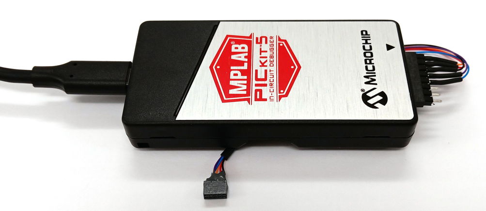
If a host board provides a programming header for an RCM6700 mounted in an mPCIe socket, this header can also be used to program an A3053 Embedded Ethernet Module plugged into the same socket. Our RCM6700 host boards are equipped with a 2×5 0.05" rectangular header, such as the GRPB052VWQS-RC. The A3053 programming signals appear on this header, and we can connect them to a Microchip ICSP programming cable with the help of an adaptor. The ICSP programming cable expects a 0.1" 1×6 rectangular plug such as the PRPC006SACN-RC, or perhaps a 0.1" 1×8 plut such as PRPC008SACN-RC. Starting with an LPPB052CFFN-RC 2×5 receptacle to mate with the header on the mother board, we run wires to a 1×6 or 1×8 plug according to the table below. We push the 2×5 receptacle onto the host board on which we have mounted our A3053. We connect the 1×6 of 1×8 header to our ICSP programmer. In the case of the PICKit5 programmer, we will use an 1×8 plug. The 1×6 is typical of older programmers. We can now program the A3053 with the ICSP protocol
| Signal | 2×5 0.05" Socket | 1×6 0.1" Plug | 1×8 0.1" Plug |
|---|---|---|---|
| !MCLR | 5 | 1 | 1 |
| VDD | 4 | 2 | 2 |
| GND | 2 | 3 | 3 |
| PGD | 8 | 4 | 4 |
| PGC | 7 | 5 | 5 |
[18-MAR-26] We distribute the circuit diagrams and printed circuit board layout of the A3053 Embedded Ethernet Module under the GNU Public License 3.0 (GPL3) with copyright held by Open Source Instruments. When you deploy the A3053 in your own host board, the host board is not subject to the A3053's GPL3 license. Because host board uses only the electrical and physical specifications of the A3053 hardware, it is not considered a derivative design under the terms of the GPL3 license. Instead, the combination of your host board and the A3053 is an aggregate of two designs, leaving your host board free of any restriction from the A3053's GPL3 license. You are also free to incorporate the A3053 circuit directly on your own host board and use the design for free, but in this case your host board becomes a derivative of the A3053, and is subject to the terms of the A3053's copyright and license. Provided you use the derivative host board only within your own institution, the GPL3 license does not require you to distribute your own design for free. But if you distribute your derivative host boards to users outside your institute, the A3053's GPL3 license requires that you distribute the entire host board design to the public for free, in the same manner as we distribute the design of the A3053 itself.
The software we provide for the A3053 Embedded Ethernet Module is available in our P3053 repository. The majority of the files in this repository are copied from Microchip Technology's Harmony repository. We have copied roughly two hundred files in all, and they are all stored in the P3053 repository's "src/microchip" directory. All these Harmony files are covered by Microchip's Harmony software copyright. This copyright permits free use, distribution, and modification of the files, but stipulates that all files must retain their original Microchip copyright notice near the top. Furthermore, the Microchip copyright prohibits the transfer of Harmony source code from the Microchip copyright to an open-source license. Almost all the Harmony files in our P3053 repository are identical to those we originally downloaded, but a few we have modified in small ways. All the files retain the original copyright statement. None of the Harmony files are subject to any copyright terms other than those of the Microchip copyright statement.
The top-level files in the A3053 Embedded Ethernet Module's P3053 code repository are written and copyrighted by Open Source Instruments Inc. These top-level files are visible in the repository's "src" directory. We distribute these files under the GNU Public License 3.0 (GPL3) a copy of which is included in the P3053 repository. The GPL3 license permits free use and modification of the software, but stipulates that any distribution of binaries compiled from GPL3 code must be accompanied by distribution of the entire body of source code from which the binaries were derived. Thus the GPL3 license permits you to modify GPL3 code, link to GPL3 code, and use the compiled binaries within your own institution without distributing your source code, but as soon as you distribute the compiled binaries to users outside your institution, the GPL3 license demands that you distribute your entire code repository under the same GPL3 license. While this GPL3 demand is perfectly acceptable to us at Open Source Instruments Inc, where everything is open-source, it will be unacceptable to many potential users of the A3053. These users need a way to deploy the A3053 on their own proprietary host boards without making their softare public.
The P3053 code repository is a detailed, complete, and accurate presentation of how to combine the A3053 Embeded Ethernet Module's PIC32MZ processor, LAN8720A physical interface, and Harmony TCP/IP stack to produce a fast TCP/IP server that manages a high-speed host board interface. The repository contains a production-ready, general-purpose TCP/IP server state machine, a Telnet server, and a high-speed parallel host board interface. There are several useful debugging and control functions available through the P3053 repository's command-line interface that will facilitate deployment of the A3053 on a new host board. While adapting the P3053 code to your own host board you are under no obligation to distribute your source code, so long as you do not distribute your compiled binaries to users outside your institution. But when it comes to distributing your host board with an A3053 running your compiled binaries, the GPL3 license demands that you either distribute all your source code under the GPL3 license, or that you replace all the GPL3 code in your repository with code you have written yourself. This latter option is the one we recommend for private companies that do not wish to release their source code. Once you have adapted the P3053 code to your own host board, replacing the P3053 repository's GPL3 code with your own code will not be difficult. Your distributed binaries will not need to use all the routines we provide in our GPL3 libraries, so replacing our GPL3 code will most likely simplify your repository while at the same time freeing it from the demands of the GPL3 license. You will certainly be linking to the Microchop Harmony libraries, but these Harmony files are covered by a copyright that permits you to compile and distribute binaries without distributing your source code. If you want to maintain a local diagnostic version of your code that uses our Telnet server, command-line interface, and server state machine, you are always free to do so within your own institution. In principle, you can turn on and off your use of our GPL3 code with your Makefile. You compile a debugging version for in-house diagnostics using one Makefile target name, and you compile a GPL3-free binary for distribution on your host boards with another Makefile target name.
[09-MAR-26] For design files and a chronological account of the development of the A3053 Embedded Ethernet Module, see its Design page.