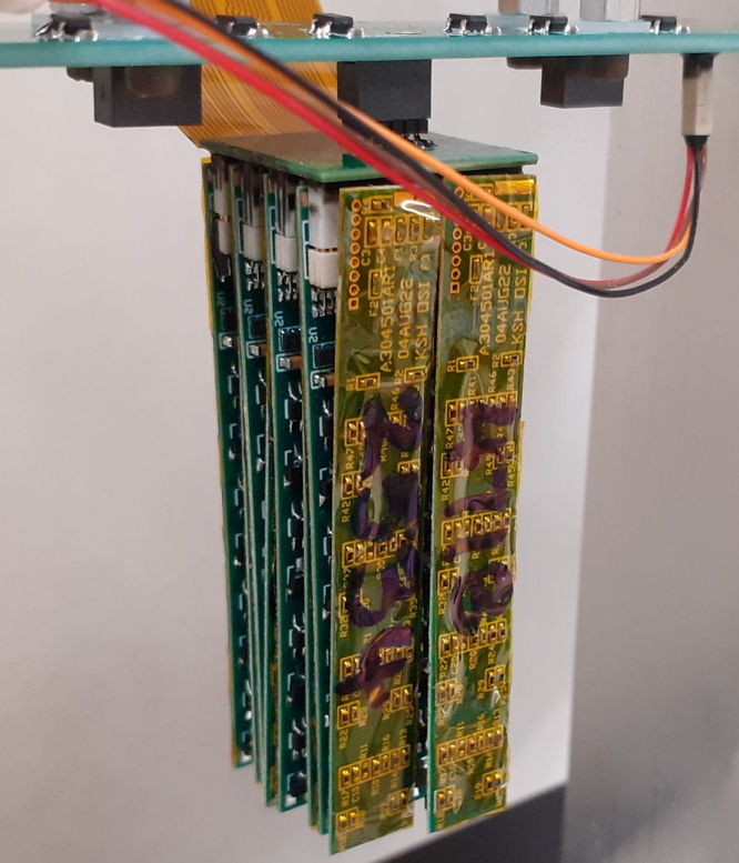
[07-FEB-23] The Direct Fiber Positioning System (DFPS) Controller (A3045) is a rectangular circuit that generates the control voltages for a single two-axis fiber positioner. The board takes as input ±250 V, 0 V, and 3.3 V power supplies and two single-ended 3.3-V logic levels Serial Clock (SCK) and Serial Data In (SDI). For outputs it has ±250-V control voltages North (VN), South (VS), East (VE), and West (VW) as well as a single-ended 3.3-V logic level Serial Data Out (SDO). The A3045 is designed to plug into a service board such as the DFPS Base and Service Board (A3043).

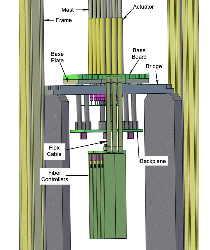
The fiber controller could, in principle, be deployed in a fiber positioning system of any size. Our prototype design deploys sixteen A3045As in a 4×4 array, as shown below.
Each controller holds four high-voltage amplifiers with gain ×200 and output range ±250 V. These are the same discrete-transistor amplifiers use in the A2089E. The amplifier inputs are driven by four slow digital to analog converters (DACs) with 0.1% precision. The DACs are driven by the controller logic, which communicates with the backplane through the service board over a two-wire bus. The controllers are identical assemblies except for their identification numbers, which allow them to be selected individually over the backplane.
The DACs perform their digital to analog conversion by low-pass filtering a square wave of variable duty cycle. Thus each DAC consists of a counter, a logic output, and a low-pass filter. Aside from the DACs, the A3045's logic chip is host to an OSR8 microprocessor and a serial command receiver.
The following versions of the DFPS Fiber Controller (A3045) are defined.
| Version | Service Board | Dimensions | Comment |
|---|---|---|---|
| A3045A | A3043A | 56 mm × 8.7 mm × 1.9 mm | Single-fiber controller with 12-way connector. |

[04-MAY-22] We arrange components on the A304501A printed circuit board: four high-voltage amplifiers, logic, and oscillator. We have plenty of space with a 60-mm long, 9-mm wide board, provided we can place P0402 resistors on the bottom side. These resistors are 0.35 mm high. We drop the board thickness to 0.53 mm (0.021"). We plan to stiffen the boards with an epoxy coating, and we will try to mount capacitors perpendicular to the board length so they do not crack when the board flexes during assembly. Our SOT-23 transistors are 1.1 mm high. In our arrangement on the service board, we have 2.6 mm between the top sides of A3043A boards, and we need 2.2 mm for two sets of SOT-23 transistors, so we have 0.4 mm clearance. The bottom sides of neighboring controller boards are separated by 1.1 mm. We need 2 × 0.35 mm = 0.7 mm for two sets of P0402 resistors or low-profile capacitors. We have 0.4 mm clearance.
[18-JUL-22] There is a third region on the circuit board: beside the connector on the top side. In this region, we have 0.8 mm clearance to the connector on the neighboring controller. We can place P0402 resistors here on top and bottom side.
[27-JUL-22] We are trying to choose the oscillator for the A2045A. The SiT1579 is a remarkable device: at 1 MHz it consumes less than 20 μA. But its package is a ceramic BGA-4 that has given us a lot of trouble in the past, when we used it on implantable transmitters. For a long time we had this device hand-placed to avoid cracking it, because it would otherwise fail more than half the time during assembly. We also had them fail by corrosion during implantation even when hand-placed. As we discussed earlier, we can make do with a 200 kHz clock on the A2045A to drive duty-cycle, ten-bit DAC. Although 200 kHz oscillators with sufficiently low current consumption do exist, they are not available for purchase during this semiconductor shortage, nor will they be available for months.
[29-JUL-22] To the first approximation, a 1% change in our low-voltage power supplies will result in a 1% change in our electrode voltages. If we want our fiber tip to be stable to 10 μm in a 3.8-mm range, the power supply must be stable to better than 0.3%. We resolve to generate on the backplane 0.01% stable 2.50 V and 1.25 V power supplies that we will distribute to all controllers. These power supplies will be fused on the controller with a 50-mA fuse. We will run the controller's OSR8 processor off a 32.768 kHz micropower oscillator, and we will run continuously a ring oscillator in the logic that will consume 1 mA from 1.25 V, which is 1.25 mW. We divide down the ring oscillator to roughly 1 MHz to duty our duty-cycle DAC. One gate switching at 1 MHz consumes roughly 10 μA, and we are going to implement four 12-bit DACs, so we expect another 240 μA to flow to the DACs. We hope to limit the low-voltage power consumption to 2 mW.
[01-AUG-22] We complete the design of the A3045AV1 circuit. We have elminated the two regulators and the high-frequency oscillator, leaving a 32.768 kHz oscillator to act as timing for incoming and outgoing communication. This communication will use the same protocol as our implantable stimulators. It is one-wire each direction, and the wire can be shared among any number of receivers. We route one of the amplifiers with its duty-cycle DAC in a 10.0 mm × 8.3 mm area. Our A304501A layout is 56 mm × 8.6 mm (2.20 in × 0.34 in), slightly smaller than the 60.0 mm × 9.0 mm permitted by our drawings, allowing us 0.2 mm thickness of epoxy on the long edges. We must cover the circuit board with something non-conducting and tough or else we will not be able to pack them next to one another without a risk of shorting the power supplies. We are using five layers, 5-mil tracks, and 8-mil via holes. Assuming four FR4 layers of equal thickness, and finished thickness 21 mil, each layer of FR4 will be around 125 μm. The breakdown voltage of FR4 is 20 kV/mm, so we don't expect breakdown between layers until around 2.7 kV and we have at most 0.5 kV between layers.
[03-AUG-22] We are able to run all connections to the WLCSP-25 along the top layer, provided we can run diagonal tracks between the pads. The balls are on a 16-mil pitch. With 5-mil tracks we have 4-mil clearance between the diagonal tracks and the edges of the balls.

By using only the top layer, we avoid needing microvias from the pads to the middle copper, which will speed up production of the board and reduce its cost.
[08-AUG-22] Fiber controller printed circuit boards are on their way, A3045 with solder paste stencil.
[24-AUG-22] We have our A304501AR1 printed circuit boards as well as a stencil. We apply paste with the stencil and load the three components that are most difficult to load by hand: J1, U1, and U2. So far as we can tell, J1 is impossible to load by hand. In the oven, J1 and U2 reflow perfectly. But we see balls under U1, the 0.4-mm pitch WLCSP-25, are joined. We remove U1 and load another by hand, using a solder blob on the top side, a 650F iron, and 20 s. We load C3 and C4. We connect 2V5 and 1V2 to 1.2V with 0.7-mm diameter SCT leads. These leads are stainless steel coils insulated with silicone.

Our task now is to program the logic chip through the SIP1MM-8. We construct an adaptor for the 1-mm pitch plug using our 0.7-mm diameter SCT leads.

With our adaptor and 1.2 V applied to both power supplies, we are able to scan U1 correctly, but we cannot program the chip. The resistance of our SCT leads is 6 Ω/cm. Our power supply leads are each 40 mm long, so we have roughly 50 Ω in series with our 1.2-V power supply. During programming, current gets as high as 20 mA, which will drop 1 V with our leads, so programming is impossible.
[25-AUG-22] We reduce the length of our 1.2-V supply lead to 1 cm and connect 0V directly to the PCB's ground pad. We are still unable to program the logic chip, we get an "OTP bit set" error. Replace the chip. Get same error. Check programming cable with an A3041A and it works fine. Go back to A3045. Forget to turn down power supply from 2.7 V to 1.2 V. We check "Progam Pin Connecte" in the programming software. We are able to program the chip. We notice our power supply error half-way through. Supply 2.5 V to 2V5 and 1.2 V to 1V2 and see 77 μA on 1V2 and 220 μA on 2V5. We try to re-program with these power supplies and get the same "OTP bit set" error. Increase 1V2 to 2V3 and all goes well. We remove our 1V2 and 2V5 supply leads. Their resistance is 7 Ω and 11 Ω respectively.
[26-AUG-22] We use copper wire to deliver 1V2 and 2V5. Our programming cable adaptor leads are 25 mm long. Resistance is roughly 15 Ω each. We can scan and erase the logic chip with 1.2 V and 2.5 V applied to 1V2 and 2V5 respectively, but we are unable to program and verify the device. We try applying 2.5 V to both 1V2 and 2V5. Scan and erase succeed but programming fails. We drop 2V5 to 2.0 V. Scan, erase, and programming all succeed. We restore 2V5 to 2.5 V. We have 69 μA flowing into 1V2 and 250 μA flowing into 2V5. This turns out to be because TP4=2V5 and we have current flowing through R4. Reprogram and 1V2 current is 69 μA while 2V5 current is 2.5 μA for 2V5 = 1.2 V and 4.5 μA for 2V5 = 2.5 V. We get the CPU running and enable the ring oscillator. We have 489 μA flowing into 1V2.
Firmware P3045 V1.2 has ND, SD, ED, and WD provided by duty cycle digital to analog converters (DACs). Software sets a two-byte value for each electrode output. We have our ring oscillator running and from it we derive Digital to Analog Converter Clock (DCK), nominally 10 MHz, as set by fck_divisor in ROM.asm. With fck_divisor = 8 we measure DCK = 10.9 MHz. A counter running on DCK counts from 0-65535 in steps of dac_step, also set by ROM.asm. With dck_divisor = 1 we measure 166 Hz. With dac_step = 8 we measure 1.2 kHz. With dac_step = 1 our resolution is sixteen bits, but the time constant of the low-pass filter that completes the digital to analog conversion will have to be 1/166 Hz × 65536 = 394 s if we are to capture our sixteen-bit resolution. With dac_step 8, our time constant need be only 1/1328 × 8192 = 6.2 s. The required time constant is inversely proportional to the square of dac_step. Our required resolution is 5 μm over a 5-mm range of motion, or 0.1%, which is 10 bits. Our required response time is of order 100 ms. The time constant will be hard-wired on the circuit board with a capacitor. The dac_step and fck_divisor we can vary with commands.

Our prototype software increments the DAC values at 200 Hz, incrementing ND, SD, ED, and WD by 1, 8, 64, and 512 counts respectively on each step. The duty cycle increases from 0% to 100 % in 328 s, 41 s, 5 s, and 0.6 s respectively. We have DCK on TP3. Current consumption is 610 μA from 1V2 and 160 μA from 2V5. We have 2V5 = 2.5 V during operation and 2.0 V during programming. Total power dissipation of the logic is 1.1 mW.
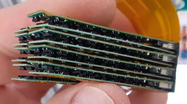
[23-SEP-22] We add logic chips to our two fully-assembled A3045As. All other parts were loaded onto paste and reflowed in our oven. Photograph of top and bottom sides here.
[05-OCT-22] We load an A3045A onto a partially-assembled Base and Service Board A3043A. We wire 1V2, 2V5 and 0V to 1.2 V, 2.0 V, and 0 V respectively and program. We repeat with our second fully-populated A3045A and program. We set 2V5 = 2.4 V. We have 650 μA flowing into 1V2 and 16 μA flowing into 2V5. We watch the duty cycle of ND, SD, ED, and WD increasing from 0% to 100% and dropping back to 0%. Frequency is 1.43 kHz. Second A3045A and current is 600 μA from 1V2 and 160 μA from 2V5. The DAC frequency is 1.38 kHz.
[06-OCT-22] Connect ±250 V to our A3043A through two 100 kΩ resistors that we can use to measure current, plug in an A3045A. See 47 μA flowing through −250V and 0.0 μA through the high-voltage ground line, implying that we have 47 μA through +250V as well. Second A3045A: 47 μA again. See schematic, we expect 2 μA through R13 and R14. Assuming high gain in Q11 and identical base-emitter voltage drop, we would get 4 μA in R15, which is currently 180 kΩ compared to R14 of 390 kΩ. But we appear to have 8 μA in R15, making a total of around 48 μA.
Our ND duty cycle varies from 0 to 100% with amplitude 2.4 Vpp. Ignoring current into U10-2, we expect U10-2, the base of the positive input transistor, to be 0.2 V to 2.2 V. Output voltage N, assuming gain of 200, should be (0.2-1.2)×200 = −200 V to (2.2-1.2)×200 = +200 V. Instead we see −100 to +190 V. We are using a ×100 probe with input impedance 100 MΩ, so the 8 μA available in R15 should be sufficient to drive N to either rail. We have 200 kΩ in series with each supply: 100 kΩ at the source and another 100 kΩ (R1 and R2) on the controller itself. With 47 μA quiescent current, the supplies drop to ±240 V. Our input NPN transistors are PMBTA42DS. At 1 μA collector current their gain is no more than 100, so we have input bias of 10 nA, which drops 50 mV across R17, which is currently 5.0 MΩ. Amplified by 200, this offset becomes 10 V.
We change R17 to 2.0 MΩ. We now see ±220 V on N, but the output jumps from −220 V to −160 V as we increase ND from 0%. The op-amp is latching down with Q11 in saturation. We did not see such saturation with the A2089E, in which the output transistor quiescent current was 14 μA, our load was 30 MΩ, and the resistor in place of R12 was only 390 kΩ.
[07-OCT-22] We load 100 kΩ for R15, R25, R35, and R45. Total ±250 V current is now 64 μA. Our output stage quiescent current is 12 μA. We see no jumps in output potentials as we ramp our DACs up and down. The ranges of signals NA, SA, EA, and WA are 0.3-1.9 V. We change schematic to show 100 kΩ for R15, etc. and 2.0 MΩ for R17, etc. We update both our A3045A. We break off one socket on our service board. We load two more and plug in both our controllers. Quiescent current is 120 μA. Total current per amplifier is 15 μA. High voltage delivered to the controllers is ±238 V (100 kΩ source resistor and 120 μA). On each controller we have R1 and R2 with 60 μA, dropping the ±250V supplies at the amplifiers to ±232 V. With 100 MΩ probe load, we see electrode voltages swings ±200 V. We have 10 MΩ output resistor on each amplifier, so saturation should be 100 ÷ 110 × ±232 V = ±211 V.

[10-OCT-22] We applied epoxy to the base of both connectors on the service board. The connectors are now firmly attached, but the epoxy interferes slightly with the fiber controller boards during insertion. But we can still load both board.
[19-DEC-22] Our resistors R11 = 5 MΩ and R17 = 2 MΩ are mismatched with respect to the input bias current of our input transistors. We would like them to be the same. The gain of the amplifier with R17 = 2 MΩ and R18 = 1 GΩ is ×500 which is excessive. The resistors in series with the ±250V power supplies on each controller are R1 = R2 = 100 kΩ, which each drop 6 V. Our output resistor R19 = 10 MΩ is designed to reduce current out of the amplifier in case of a short, but will drop out output voltage by 10% when viewed with a 100-MΩ probe. We see only ±200 V with the probe when we expect ±211 V.
[20-DEC-22] To provide SDI and receive SDO we are re-programming a Command Transmitter (A3029), disabling all the RF amplifiers and the SAW oscillator, and soldering our cable to suitable points on the top side, creating the A3029F. We prepare firmware P3029F for the A3029F. Communication between the command transmitter and the fiber controller will follow the slow serial protocol we use in our Implantable Stimulator-Transponders (A3041).

[21-DEC-22] We implement the following instructions in our fiber controller assembly program. We implement all instructions, but we have dummy procedures for shutdown, acknowledge, and identify. The missing opcode 7 is an oversight. We have not yet decided the SDO protocol, so we cannot implement acknowledge or identify.
| Instruction | Opcode | Operands | Function |
|---|---|---|---|
| shutdown | 0 | none | Undefined |
| north | 1 | 2 bytes: HI and LO | set the north electrode potential |
| south | 2 | 2 bytes: HI and LO | set the south electrode potential |
| east | 3 | 2 bytes: HI and LO | set the east electrode potential |
| west | 4 | 2 bytes: HI and LO | set the west electrode potential |
| acknowledge | 5 | none | transmit self identifier immediately |
| identify | 6 | none | trasmit self identifier after unique delay |
| selftest | 8 | none | run a ramping-voltage self-test |
The self-test is the same procedure we used to check the dynamic range of the fiber controller outputs earlier. We start the self test with a command ending in a selftest instruction. We end it with any other command, even an empty command. The fiber controller recognises its own identifier and the wildcard identifier 0xFFFF, so we can send commands to all controllers or to one individual controller. We connect our Command Transmitter (A3029F) to a Backplane (A3044A), into which we plug a Base and Service Board (A3043A) fully populated with pins and plugs. We plug one Fiber Controller (A3045A) into one of the plugs.

We use the Stimulator Tool to send commands to the A3045. After fixing some bugs, command reception works perfectly. We can set the electrode DACs, we can start and stop the self-test.
[27-DEC-22] With each of our amplifiers consuming of order 20 μA, resistors R1 and R2, now 100 kΩ, will drop 8 V each, reducing our high-voltage power supply from ±250 V to ±242 V. These resistors are intended to protect the system from a short circuit within the A2045. We drop their values to 10 kΩ and trust that no short circuit will occur spontaneously on the A3045 circuit board. Short circuits from the electrode outputs N, S, E, W will do no harm because they are mitigated by 10-MΩ series resistors Rn9. We do not need R11, now 5 MΩ. Voltage ND comes from a logic output, which provides a DC path to ground for U10-2. We remove all four Rn1, marking as OMIT. Now our voltage ND has range 0.0 to 2.4 V, or ±1.2 V with respect to the 1V2 we use as the amplifier ground. We leave R10 as 1 MΩ and drop R17 from 2 MΩ to 1 MΩ. The symmetry between R10 and R17 reduces the amplifier's input offset voltage. We drop R18 from 1 GΩ to 250 MΩ, giving the amplifier a gain of 250 V. We update S3045A_1 and S3045A_2 and set about making modifications.
[29-DEC-22] We have 0xA123 with modifications described above. We apply logic LO to ND (send command 0xA1230100). We see ND = NA = 20 mV. We apply logic HI to ND (command 0xA12301FFFF). We see 2V5 = 2.30 V, ND = 2.30 V and NA = 2.26 V with our 100-MΩ probe. Noting that R10 is 1.0 MΩ, these observations are consistent with NA = ND = 2V5 = 2.4 V. We apply ±250 V power the wrong way around to A3044A P1. Capacitors C1 and C2 on A3044A blow up and short. We replace capacitors and correct connector wiring, turn off high voltage power supply, plug connector into backplane and turn on high voltage power. All is well. We apply LO to ND and see 0 mV on NA and −212 V at NB and −196 V on N with our 100 MΩ probe. We apply HI to ND and see NA = 2.2 V, Q10-1 = 252 V and N = 228 V. We vary the DAC count between 0 and 65535. At each value we record the value of Q10-1, the output before protection resistor R19. After pressing Transmit in the Stimulator Tool we wait five seconds for the output voltage to settle.

Gain with R12 = 1.0 MΩ is 201 V/V from NA to NB averaged over the entire range, but 218 V/V at the center of the range. When NA = 1.2 V we have NB = 32 V. When we place a 10-MΩ probe on NA, grounded to 0V we drop the maximum value of VA from 2.4 V to 2.2 V.
[30-DEC-22] Repeat above sweep with R12 = 390 kΩ on 0xA123. Range is now −220 V to +204 V. We record both VA and VB. Fit straight line to VB versus VA and find slope is 200 V/V with residuals 5.5 V rms. We rip P12 right off the board, pulling its tracks off as well. Cut back tracks. Apply black DP270 to the bases of the remaining 15 connectors. Program another controller with ID 0xB341 and R12 = 1.0 MΩ. Repeat sweep.

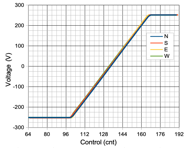
Slope of VB versus VA is 205 V/V, residual 7.5 V rms. Residual of VA versus DAC is 0.3% rms. We see some flux residue on the circuit board. Wash and dry. Repeat several measurements, they are consistent with before washing. We remove our probe from NA with DAC = 65535 and see VA jump up to 252 V. The minimum VB is still −212 V. We try R12 = 390 kΩ, which give us more symmetry, and R17 = 909 kΩ (formerly 1.0 MΩ) and see range −244 V to + 252 V. We try R12 = 390 kΩ and R17 = 620 kΩ and perform a full sweep, probe on only VB.

Here we see saturation at +252 V and −244 V according to our ×100 probe, which is accurate to around ±1%. With outputs at zero, these amplifiers should consume 12 μA. Quiescent current of the four amplifiers on one A3045 should be around 50 μA, dropping 0.5 V accross each of R1 and R2. Saturation on the negative side should be 1 V above −250V and 0.2 V below +250V. Our observations are consistent with the opamp operating correctly at its extremes.
Our feedback network R18 = 250 MΩ and R17 = 1.0 MΩ divides by G = 250. Our observed gain NB/NA ≈ 210. Let the open-loop gain of our high-voltage op-amp be A = NB/(NB/G − NA). We get NA/NB = 1/A + 1/G. For A ≫ G, these relations collapse to NB/NA = G. But in our case we have 1/A = 1/210 − 1/250 = 1/1300. It looks like the open-loop gain of our op-amp is 1300. When we have R17 = 620 kΩ, we have G = 400. We see NB change by 496 V as cnt/256 changes by 170, which implies NA changed by 2.4 × 170 / 256 = 1.6 V so NB/NA = 496/1.6 = 310. We have 1/A = 1/300 − 1/400 = 1/1200, so A appears to be 1200. Our ideal NB/NA is a little over 500 / 2.4 = 208. If A = 1000 we want G = 263, so R17 = 950 kΩ. We have ordered 910 kΩ resistors.
[01-JAN-23] We remove R18 on 0xA123 and attempt to measure open-loop gain. The op-amp latches down until cnt/256 = 130, then latches up, so we are unable to make our measurement. We measure the dynamic range of 0xB341 again and obtain the same value: −244 V to + 252 V. We measure our power supplies at the op-amp, on R12 and R13. We get −244 V and +252 V. We conclude that our op-amp's output spans the full range of the supplies.
[04-JAN-23] We load both A123 and B341 onto our service board and connect NB of each to a 10-MΩ voltmeter through a 100-MΩ resistor. The load on NB is 110 MΩ. The voltage we measure on the voltmeter is 1/11 of the voltage on NB. We assert DAC values, not increasing from zero, but jumping randomly about until we fill the entire range. On a move from -200 V to + 200 V, we observe the output settling to within 1% of its final value within four seconds, which is consistent with the 1-s time constant generated by R10 and C10. We have to wait ten seconds for the voltmeter measurement to settle to ±0.1%.

Residuals to a straight line for DAC values 10-250 cnt/256 are 7 V rms. Average difference B341−A123 is −0.5 V, standard deviation 1.8 V. Saturation is at −249.5 V and +250.8 V for both amplifiers, according to our meters. We finalize our resistor values: we will use 910 kΩ for R10 and R17, 390 kΩ for R12 and corresponding resistors in other amplifiers. We measure the voltage across R1 and R2 with no load on NB. Each fiber controller consumes 75 μA from ±250 V. We update our schematic. We proceed with modification of existing boards, and then loading logic chips to complete a total of 17 fiber controllers.
[09-JAN-23] We have four controllers with latest resistor values loaded. We measure output voltage versus DAC value for all four pole outputs of all four controllers and call this process QC1. We are using our new Fiber Controller 2.0 software to set the pole DAC values.


We are not sure about the South pole on A123. One of the modifications may have been missed for that amplifier. But we are going to leave it as it is.
[10-JAN-23] Load 100 nF for C10, C20, C30, and C40 on 0x784E. Response time constant for output poles is now 100 ms and the outputs settle in 1 s. For various output voltages, ripple at the DAC frequency is less than 50 mV (cannot see any DAC ripple with our 100 mVpp noise). The faster time constant makes measurement easier. We can now run a travel script in the Fiber Positioner and step through all QC1 positions in twenty seconds automatically, with full settling at each step.
[26-JAN-23] We load the backplane onto the underside of our bridge, connect logic signal and power, plug our service board into the backplane, and plug a single fiber controller into the service board. We connect ±250 V to the backplane. We hear a spark. We have only ±225 V on the backplane until we unplug the controller, after which we see the full ±250 V. We have loaded the backplane the wrong way around. The service board plug is not polarized, so we plugged it in rotated 180°. The table below gives the signals on the backplane and the signals they were connected to on the single fiber controller.
| Backplane | Controller |
|---|---|
| −250V, Pin 1 | 2V5, Pin 10 |
| NC, Pin 2 | 0V, Pin 9 |
| +250V, Pin 3 | SDI, Pin 8 |
| NC, Pin 4 | 1V2, Pin 7 |
| NC, Pin 5 | SDO, Pin 6 |
| SDO, Pin 6 | NC, Pin 5 |
| 1V2, Pin 7 | NC, Pin 4 |
| SDI, Pin 8 | +250V, Pin 3 |
| 0V, Pin 9 | NC, Pin 2 |
| 2V5, Pin 10 | −250V, Pin 1 |
The three unused pins do not overlap when we rotate, so there are only four electrical connections to the controller. The controller's 2V5 is being held at −250 V. The controller's SDI is being held at +250 V. The SDI signal passes through 10 kΩ on its way to the logic chip. We will have at least 25 mA flowing into the logic chip input. Damage is likely. The controller's ±250V supply is being driven by the backplane's SDI and 2V5. No more than a few microamps can pass out of the amplifiers. We doubt the backplane has suffered any damage.
[07-FEB-23] We have eleven programmed fiber controllers. Serial numbers are 784E, B341, 2534, C323, 4718, D729, 1834, 6912, 1845, A123, and E381. We use our QC1 Travel Script to move each voltage from its negative to positive extreme in steps. We check that every amplifier is responding correctly. It takes us a full day to debug the circuits. We blow up two more in the process. We have four more controllers that are not programmed, nor checked, but have logic chips loaded. We load them all onto a service board.
We operate each controller individually with no difficulty using our Fiber Controller software. We leave the high-voltage power on all day, moving the positioners back and forth along a diagonal of their dyna ic range. The positioners are still moving just fine at the end of the day.