| Description |
| Ordering |
| Versions |
| Analog Inputs |
| Battery Voltage |
| Battery Life |
| Implantation |
| Synchronization |
| Encapsulation |
| Design |
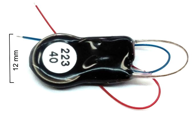
[10-APR-26] The A3048 Subcutaneous Transmitter (SCT) is an implantable telemetry sensor for small animals. It provides amplification and filtering of a single biopotential input. When equipped with a CR927 battery its mass is only 1.5 g. All versions of the A3048 operate within our Telemetry System. All versions turn on and off with a magnet.
The amplifier on the A3048 Subcutaneous Transmitter can provide gain of ×100 for frequencies up to 160 Hz, or it can provide gain of ×25 for frequencies up to 640 Hz. The A3048 logic may be programmed to sample at 64, 128, 256, 512, 1024, or 2048 SPS. The low-pass filter may be configured for a corner frequency of 20, 40, 80, 160, 320, or 640 Hz. The high-pass filter can be configured to for a corner frequency of 0.2 Hz or 2 Hz, or it can be removed entirely to allow the amplifier to provide gain all the way down to 0.0 Hz (DC). All versions of the A3048 are equipped with flexible red and blue leads and a loop antenna. The length of the leads, the size of the battery, the operating life, the termination of the leads, the sample rate, the gain of the amplifier, and the passband of the amplifier vary from one version to the next.
| Property | Specification |
|---|---|
| Volume | 0.95±0.1 ml |
| Mass | 1.9±0.1 g |
| Operating Life | 41 days |
| Battery Capacity | 2000 μA-days |
| Shelf Life | 6 months |
| On-Off Control | magnet |
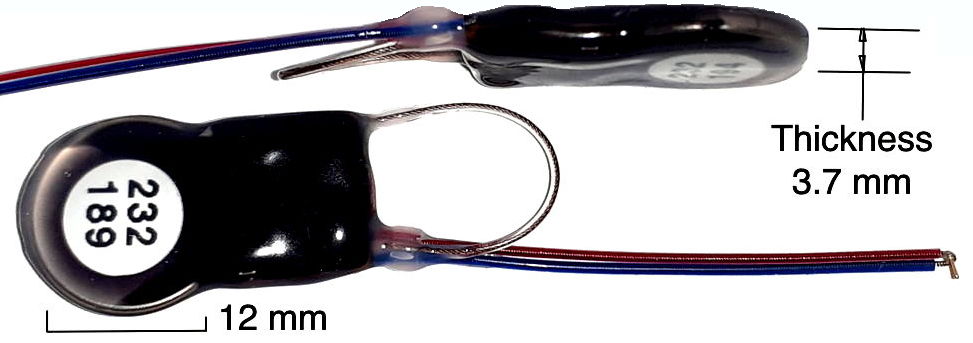
| Lead Dimensions | diameter 0.5±0.1 mm, length 50±2 mm |
| Lead Terminations | steel coil, diameter 0.25 mm, length 1.0 mm |
| Number of Inputs | 1 |
| Input Impedance | 10 MΩ |
| Sample Rate | 256 SPS |
| Bandwidth | 0.3-80 Hz |
| Noise | ≤3 μV rms |
| Distortion | <0.1% |
| Dynamic Range | 30 mV (−18 mV to +12 mV) |
| Resolution | 16-bit |
| Absolute Maximum Input Voltage | ±3 V |
All A3048 Subcutaneous Transmitters transmit on a single telemetry channel. Each transmitter has a label under its silicone coating. Thius label specifies the batch number, B, and the telemetry channel number, N. All versions of the A3048 are covered by a one-year warranty against corrosion and manufacturing defect.
[06-JUN-25] There are many possible configurations of the A3048 Subcutaneous Transmitter. Each configuration becomes an established "version" when we manufacture it for a customer. We list the available A3048 versions in the section below. You will find our latest prices in our Price List. To determine which SCT is best for your application, feel free to consult the OSI Chatbot. To obtain a quotation for manufacture and delivery, or to ask us questions directly, please email us at info@opensouresintruments.com.
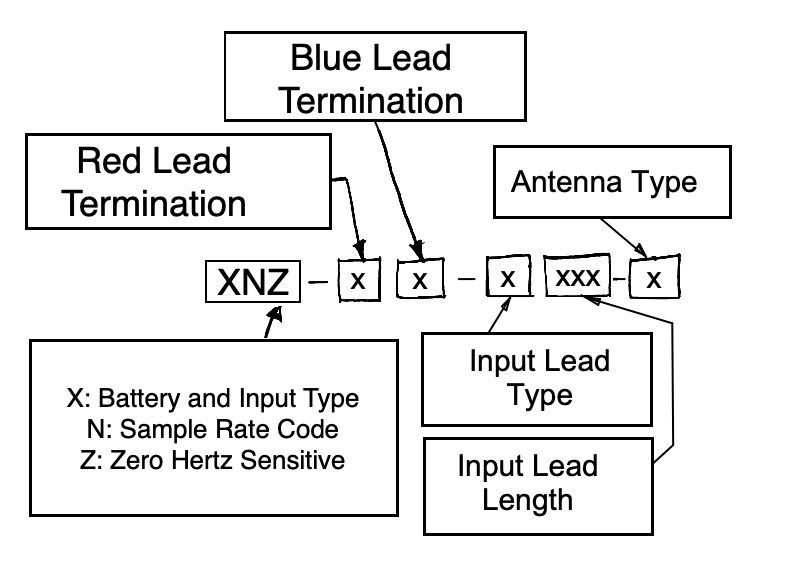
[05-JUN-26] The A3048 Subcutaneous Transmitter can be equipped with several sizes of battery and leads up to 130 mm long. It can be configured with a variety of passbands, dynamic ranges, and sample rates. You specify the version you want with a full SCT part number. The part number begins with "A2048" and is followed by the primary version letter. The primary version letter specifies the battery we load on the circuit. Following the primary version letter, we have a sample rate code number. We use the numbers 1-5 to indicate 128, 256, 512, 1014, and 2048 SPS respectively. We add the letter "Z" to indicate that the passband of the amplifier extends down to 0.0 Hz, making a "DC transmitter". If we omit the "Z", the passband begins at 0.2 Hz, making an "AC transmitter". Now comes a dash followed by letters indicating the terminations of the leads. After another dash comes a letter and a number specifying the type and length of the leads. After a final dash we have a letter specifying the antenna.
See our Electrode Catalog for a list of available lead terminations, and also for a presentation of the various depth electrodes to which these terminations can be attached. See our Leads Table for a description of our several types of insulated, coiled steel spring leads. See our Antennas table for a description of the various types of antenna we can deploy on our implants. The following versions are defined already, but we are happy to define new ones to suit your needs. The operating life is the minimum time for which a newly-made transmitter will operate continuously. The shelf life is the time the transmitter can remain turned off in storage and still retain 90% of its operating life.
| Version | Passband, Sample Rate, Dynamic Range |
Battery Capacity (μA·d) |
Volume (ml) |
Mass (g) |
Operating Life (d) |
Shelf Life (mo) |
Comment |
|---|---|---|---|---|---|---|---|
| A3048P0Z | 0.0-20 Hz, 64 SPS, 120 mV | 1000 (CR927) | 0.85 | 1.5 | 39 | 3 | Smallest, continuous-use only, CSDs |
| A3048P2 | 0.2-80 Hz, 256 SPS, 30 mV | 1000 (CR927) | 0.85 | 1.5 | 21 | 3 | Smallest, continuous-use only |
| A3048R0Z | 0.0-20 Hz, 64 SPS, 120 mV | 1250 (CR1216) | 0.90 | 1.7 | 49 | 4 | Thinnest, slow waves and CSDs |
| A3048R1 | 0.2-40 Hz, 128 SPS, 30 mV | 1250 (CR1216) | 0.90 | 1.7 | 38 | 4 | Thinnest, seizure-detector |
| A3048R2 | 0.2-80 Hz, 256 SPS, 30 mV | 1250 (CR1216) | 0.90 | 1.7 | 27 | 4 | Thinnest, ictal event monitor |
| A3048S0Z | 0.0-20 Hz, 64 SPS, 120 mV | 2000 (CR1225) | 0.95 | 1.9 | 79 | 6 | Slow waves and CSDs |
| A3048S1 | 0.2-40 Hz, 128 SPS, 30 mV | 2000 (CR1225) | 0.95 | 1.9 | 61 | 6 | Long-term seizure-counting |
| A3048S2 | 0.2-80 Hz, 256 SPS, 30 mV | 2000 (CR1225) | 0.95 | 1.9 | 41 | 6 | Epilepsy monitor |
| A3048S2Z | 0.0-80 Hz, 256 SPS, 120 mV | 2000 (CR1225) | 0.95 | 1.9 | 41 | 6 | Epilepsy, sleep, and CSDs |
| A3048S3 | 0.2-160 Hz, 512 SPS, 30 mV | 2000 (CR1225) | 0.95 | 1.9 | 25 | 6 | High-bandwidth iEEG, ECoG, LFP |
For the analog input on an A3048 Subcutaneous Transmitter, we specify the passband, sample rate, input dynamic range, and channel number offset. The passband is the range of frequencies to which the amplifier responds. The passband has a low and high end, both of which we specify in the tbale. The bandwidth of an input is the difference between the high and low ends of its passband. For all A3048 SCTs, bandwidth is approximately equal to the high end of the passband.
The dynamic range of the A3048 input is always 0-65535 when expressed in terms of the sample value we obtain from the A3048's sixteen-bit ADC. The zero-value of an input is the sample value we obtain when we short the two input electrodes together. The zero-value depends upon the battery voltage, VB, according to zero-value = 1.8 V · 65535 / VB. The dynamic range is the battery voltage divided by the gain of the amplifier. When we specify dynamic range, we assume VB = 3.0 V, which is true for almost the entire life of the lithium batteries we use with the A3048. When the amplifier gain is 100, the dynamic range is 30 mV and spans −18 mV to +12 mV.
See the Battery Life chapter of our telemetry manual for an explanation of how operating life of A3048-family SCTs varies with mass and sample rate. In almost all cases, we set the sample rate of an input equal to 3.2 · B, where B is the bandwidth in Hz. This sample rate makes it possible for the low-pass filter to provide 20 dB attenuation at one half the sample rate, which is 1.6 · B. Frequencies above one half the sample rate will be distorted by sampling, but the 20-dB attenuition ensures that such signals do not corrupt the signal we record from the SCT's passband.
We cannot use just any coin-cell battery in our A3048 Subcutaneous Transmitters. Most small coin cells are unable to deliver the pulse of current required to wake up the A3048 circuit. Even if they can provide this current pulse when they are fresh, they will be unable to do so when they are down to 10% capacity. We use CR1216 batteries from Murata, a manufacturer that guarantees current pulse performance throughout the life of all their coin cells. Murata does not make either CR927 or CR1225 batteries, so we use CR1225 batteries from Multicomp and CR927 batteries from Premium Battery. These we buy in batches of one or two hundred, from which we select five or ten examples to test for operating life and pulse performance. The Multicomp CR1225 provide reliable battery life and good pulse performance. The Permium Battery CR927 provide reliable battery life of 1000 μA·d, and is the battery deployed in our P-Series A3048 transmitter. But the pulse performance of these batteries degrades half-way through their operating life. They have difficulty powering up the A3048 circuit from sleep. The CR927 battery is not suitable as a power supply for an A3048 if we want to turn the transmitter off for a few days and then turn it on again. We say the P-Series devices are "continuous use only". If you accidentaly turn off an A3048P half-way through its operating life, tap it three distinct times with a magnet while counting one, two three. You turn it on, off, and on again. The second time you turn it on, it will most likely power up properly.
[07-FEB-25] When configured for AC recording, the input of an A3048 Subcutaneous Transmitter consists of a in series with a resistor. These together form a high-pass filter with corner frequency 0.16 Hz and input impedance 10 MΩ The most common versions of the A3048 provide a gain of ×100, another high-pass filter, and a three-pole low-pass filter. When we remove the high-pass filter, the passband of the amplifier will extend all the way down to 0.0 Hz, thus configuring the SCT for DC recording. We can configure the low-pass filter with any of the corner frequencies 20, 40, 80, 160, 320, and 620 Hz. These frequencies are matched with sampling rates 64, 128, 256, 512, 1024, and 2048 SPS respectively.
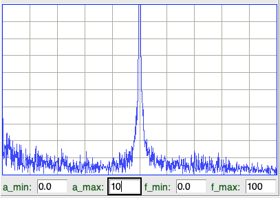
The figure below shows the frequency response of a batch of twenty-two A3048R2 transmitters recorded during Quality Control Two (QC2). You will find a database of such plots here. We send one such plot along with each batch of transmitters we ship.
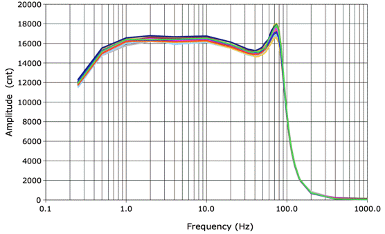
In the response shown above, we see both the high-pass filter corner frequency and the low-pass corner frequency. If we define "corner frequency" as the frequency at which the gain drops to 70% of the gain in the passband of the amplifier, the corner frequencies for this batch of transmitters are 0.2 Hz and 90 Hz. The actual bandwidth is slightly greater than the nominal 80 Hz specified for the A3048R2. The most important function of the low-pass filter is to reduce the amplifier voltage gain by at least a factor of ten at a frequency that is one half the sample rate. We see that this is indeed the case for our batch of A3048R2s. They sample at 256 SPS and their gain at 128 Hz is less than 10% of their gain at 10 Hz.
| Range (mV) | Low (mV) | High (mV) |
|---|---|---|
| 30 | -18 | 12 |
| 60 | -36 | 24 |
| 120 | -72 | 48 |
| 150 | -90 | 60 |
| 300 | -180 | 120 |
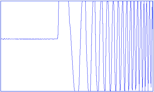
The amplifier is powered by the battery voltage, VB, which is typically 3.0 V at 37°C, but will be 3.1 V for the first 5% of the battery's life and drop below 2.6 V in the final 5%. The amplifier saturates within 20 mV of 0V and VB. The following saturating sweep response shows how well the amplifiers handle large inputs. For a comparison of the A3048S2 saturation behavior and that of its predecessor the A3028S2, see here.
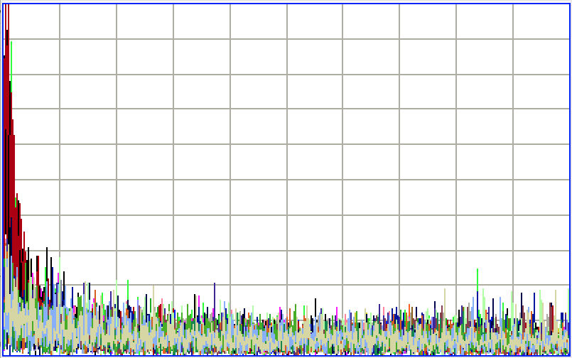
We measure the electrical noise on the A3048 input by placing the entire transmitter in water and letting it settle for a few minutes. Typical noise for an A3048S2 with 80-Hz bandwidth is 5 μV rms. The figure below shows the spectrum of electrical noise for a batch of A3048S2s.
The A3048P-series subcutaneous transmitters are equipped with a CR927 coin cell. The CR927 is 9-mm in diameter and 2.7 mm thick. When loaded with the CR927, some SCTs will exhibit switching noise of amplitude up to 2 μV rms. This noise is caused by an interaction between transmitter's magnetic switch, which turns on and off at around 5 Hz, and the source impedance of the battery, which is larger for smaller batteries. Here is the electrical noise spectrum of a batch of A3048P2s.
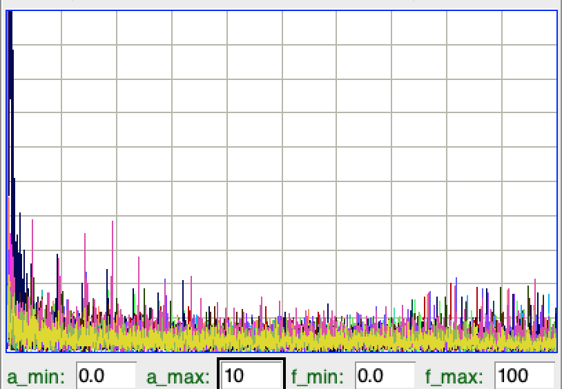
The switching noise we see in the A3048P-series transmitters consists of 10-ms pulses at roughly 5 Hz. The height of these pulses decreases with temperature. At 37°C, they will be no more than 10 μVpp, but at room temperature they can be as large as 30 μVpp. A typical EEG signal from a bare wire electrode in a mouse is 40 μV rms, 160 μVpp. Switching noise pulses of 10-μV are hard to see.
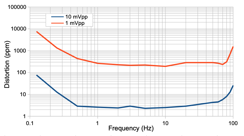
The distortion of a signal by an SCT is the extent to which the SCT changes the shape of the signal's sinusoidal components. We apply a 10 mVpp sinusoid to the input of an A3048S2, which provides 0.2-80 Hz passband and 30-mV dynamic range. We increase the frequency from 0.125 Hz to 100 Hz. For each frequency, we obtain the spectrum of the signal and measure the power outside the sinusoidal frequency as a fraction of the sinusoidal power using this script. We express the result in parts per million. The distortion of the recorded signal is dominated by random electronic noise. There are no significant peaks in the spectrum outside the fundamental.
We note that the distortion generated by the A3048 family of subcutaneous transmitters is hundreds of time less powerful than that of the discontinued A3028 family of SCTs. The A3048 samples the signal uniformly, thus eliminating the scatter noise present in the A3028 signal.
[30-JUN-25] We refer you to the Battery Voltage chapter of our Telemetry Manual for a discussion of how we can measure an A3048's battery voltage during operation.
[26-JUN-25] All A3048 Subcutaneous Transmitters are equipped with non-rechargeable lithium coin cells. The operating life of an A3048 is how long it can amplify and transmit its input voltage when starting with a fresh battery. Its shelf life is how long it can wait on the shelf in its sleep state before it has used 10% of its battery capacity. We list operating and shelf life in the A3048 Version Table. We provide a detailed discussion of SCT operating life in the Battery Life chapter of our Telemetry Manual. Here we present some tables and measurements specific to the A3048 family.
| Total Sample Rate (SPS) |
CR927 1250 μA·d |
CR1220 1650 μA·d |
CR1225 2000 μA·d |
CR1620 3300 μA·d |
|---|---|---|---|---|
| 64 | 49 | 65 | 79 | 131 |
| 128 | 38 | 50 | 61 | 102 |
| 256 | 26 | 35 | 42 | 70 |
| 512 | 16 | 21 | 26 | 43 |
The above table of operating life shows how sample rate and battery capacity dictate operating life. The table gives the minimum operating life of a newly-made transmitter. The average operating life is roughly 5% higher, and in some cases even higher. We recently saw an A3048S2 with minimum operating life 41 days run for a full 50 days before stopping.
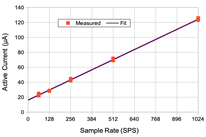
The active current consumption of A3048 increases linearly with sample rate, but also varies from one A3048 to another. For each version of the A3048, there is a maximum active current that we will accept during quality control. The minimum operating life of this version is its nominal battery capacity divided by its maximum active current. To see how we calculate the maximum active current of a particular A3048 version, see the Battery Life chapter of our Telemetry Manual.
[17-JUN-25] See the Implantation chapter of our Telemetry Manual for a presentation of implantation procedures and protocols. The A3048 family of subcutaneous transmitters are single-channel only, but they are small enought to implant along with an implantable stimulator for simultanous, wireless, stimulation and biopotential monitoring.
[17-JUN-25] When we want to mark in our recordings the time at which some event took place, such as the start of a video recording or the moment a light was flashed, we can use an auxiliary SCT to add a synchronizing signal to our recording. See the Synchronization chapter of the Telemetry Manual for details.
[29-NOV-23] All versions of the A3048 are encapsulated in black epoxy and coated with silicone. The silicone is "unrestricted medical grade" MED-6607, meaning it is approved for implants of unlimited duration in any animal, humans included. The A3048's leads and antenna are encapsulated with dyed silicone, then coated with the same unrestricted medical grade silicone. The only materials the transmitter and its leads present to the subject animal's body are either unrestricted medical grade silicone or stainless steel.
[09-JUN-25] For design files and development logbook, see the A3048 design and development page at D3048.