| Description |
| Ordering |
| Versions |
| Analog Inputs |
| Battery Voltage |
| Battery Life |
| Implantation |
| Synchronization |
| Encapsulation |
| Design |
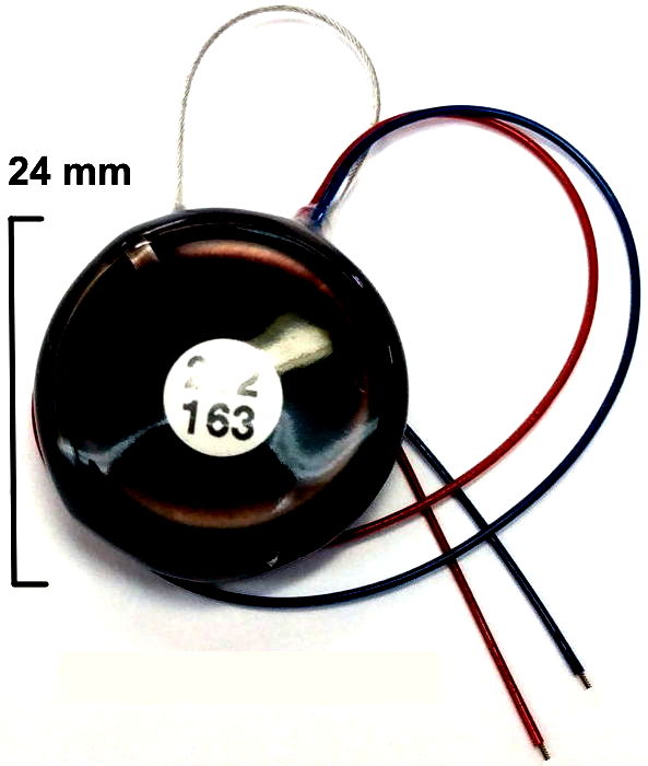
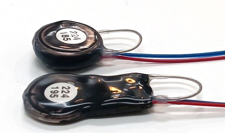
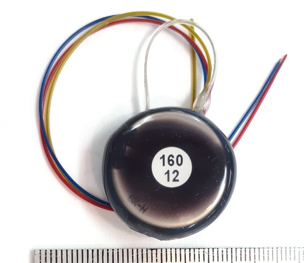
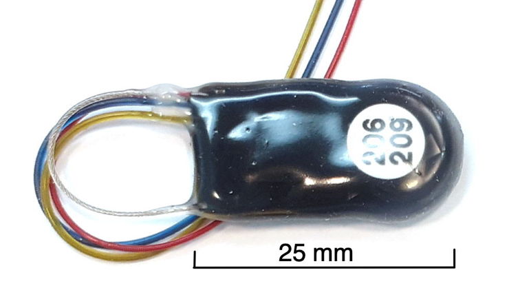
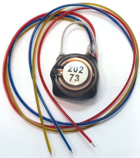
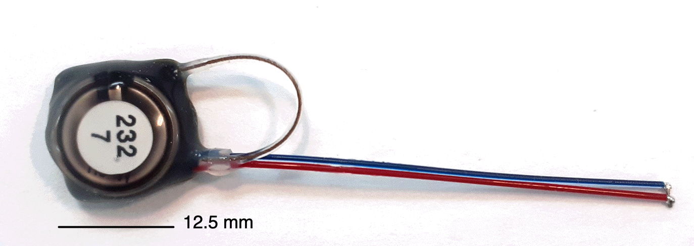
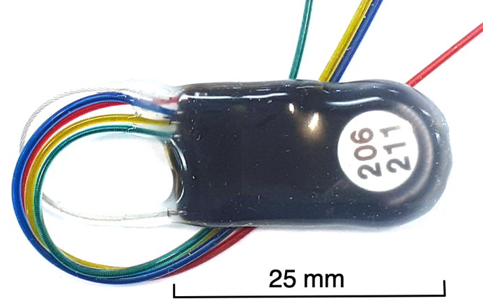
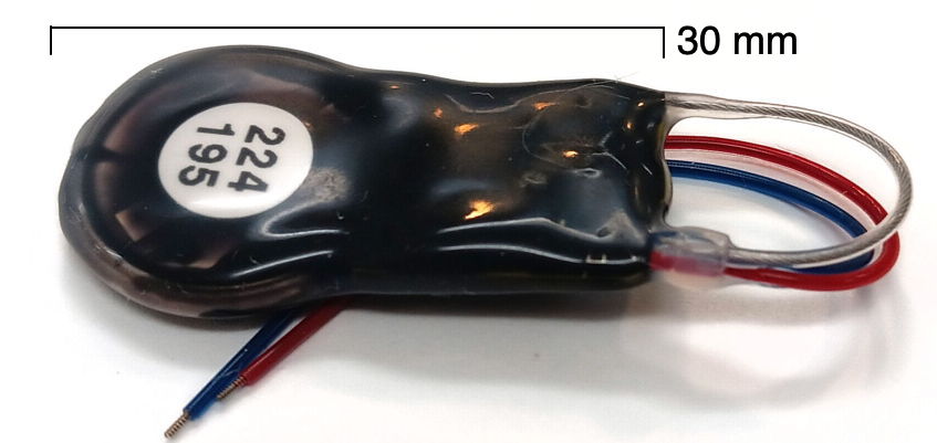
[07-JUL-26] The A3049 Subcutaneous Transmitter (SCT) is an implantable telemetry sensor for small animals. It provides amplification and filtering for two independent biopotentials. When equipped with a CR1220 coin cell, its mass is only 2.0 g, making it suitable for implantation 20-g mice. When equipped with a CR2477 coin cell, its mass is 14 g, making it suitable for implantation in large rats. All versions of the A3049 operate within our Telemetry System. All versions turn on and off with a magnet.
The amplifiers on the A3049 Subcutaneous Transmitter can be configured to provide gain of anywhere from ×10 to ×100. Their low-pass filters can be configured with a corner frequency of 20, 40, 80, 160, 320, or 640 Hz. Their high-pass filters can be configured with a corner frequency of 0.2 Hz or 2 Hz, or the high-pass filter can be removed entirely to provide gain all the way down to 0.0 Hz (DC). The A3049 logic can be programmed to sample at 64, 128, 256, 512, 1024, or 2048 SPS, so as to suite the corner frequency of the low-pass filter. All versions of the A3049 are equipped with flexible leads and a loop antenna. The length of the leads, the size of the battery, the operating life, the termination of the leads, the sample rate, the gain of the amplifier, and the passband of the amplifier vary from one version to the next.
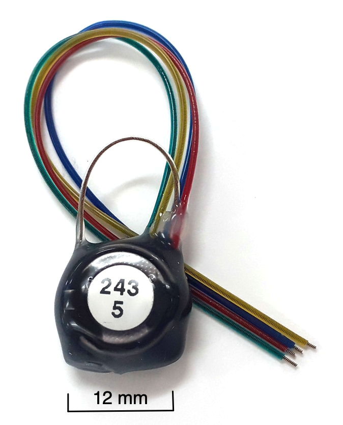
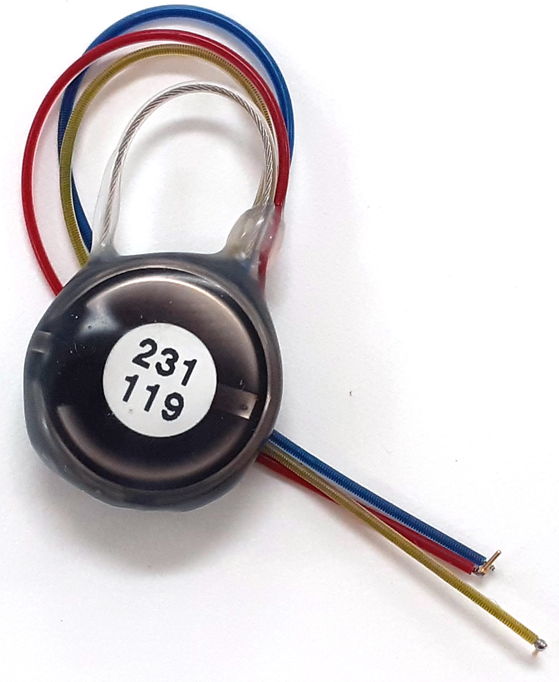
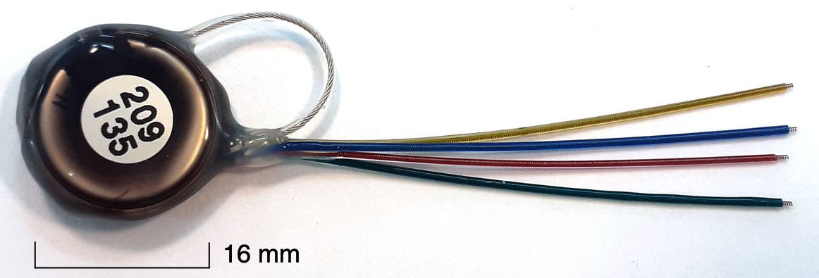
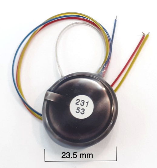
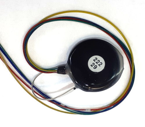
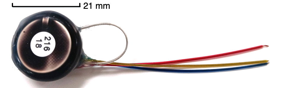
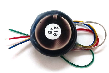
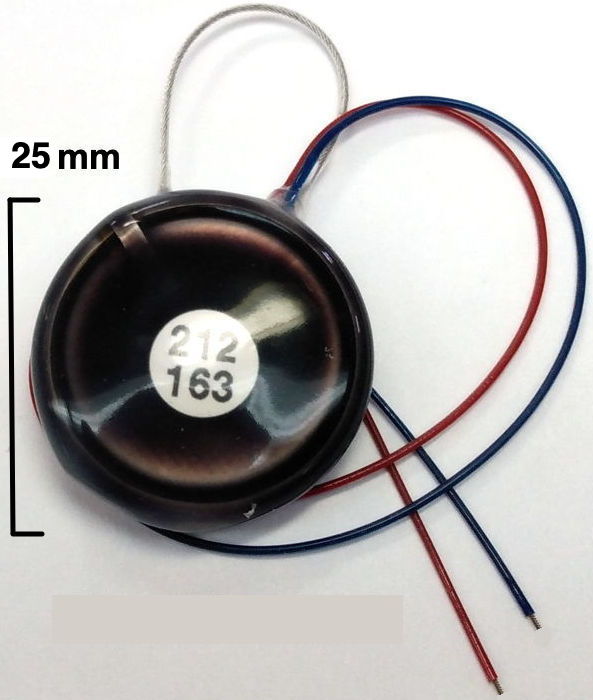
The A3049 Subcutaneous Transmitter can be configured to provide either one or two inputs. The two inputs can share a common reference potential or they can each have their own reference potential. A one-input sensor will transmit one signal on one telemetry channel. As a two-input sensor will transmit on two telemetry channels. The color and number of leads loaded on the transmitter depend upon its input configuration.
| Type | Input Configuration | X+ | X− | Y+ | Y− | Applications |
|---|---|---|---|---|---|---|
| I | One Input, X Amplifier | Red | Blue | Omitted | Omitted | EEG, EMG, ECG, or EGG |
| II | One Input, Y Amplifier | Omitted | Omitted | Yellow | Green | none |
| III | Two Inputs, Common Reference | Red | Blue (Shared) | Yellow | Blue (Shared) | EEG+EEG |
| IV | Two Inputs, Separate References | Red | Blue | Yellow | Green | EEG+EMG, EMG+EGG, EEG+ECG |
Each transmitter has a label under its silicone coating. This label specifies the batch number, B, and the first channel number, N. A one-input transmitter uses channel N only. A two-channel transmitter uses channel N for the X input and N+1 for the Y input. In a two-channel transmitter, N is always odd.
| Property | Specification |
|---|---|
| Volume | 1.2±0.1 ml |
| Mass | 2.2±0.1 g |
| Operating Life | 14 days |
| Battery Capacity | 2000 μA-days |
| Shelf Life | 6 months |
| On-Off Control | magnet |
| Input Configuration | III, Dual-Input, Common Reference |
| Lead Dimensions | diameter 0.7±0.1 mm, length 45±2 mm |
| Lead Terminations | steel coil, diameter 0.45 mm, length 1.0 mm |
| Input Impedance | 10 MΩ |
| Sample Rate | 512 SPS each channel |
| Bandwidth | X: 0.16-160 Hz, Y: 0.16-160 Hz |
| Noise | <6 μV rms |
| Distortion | <0.1% |
| Dynamic Range | 30 mV (−18 mV to +12 mV) |
| Resolution | 16-bit |
| Absolute Maximum Input Voltage | ±3 V |
All versions of the A3049 Subcutaneous Transmitter are covered by a one-year warranty against corrosion and manufacturing defect.
[06-JUN-25] There are many possible configurations of the A3049 Subcutaneous Transmitter. Each configuration becomes an established "version" when we manufacture it for a customer. We list the available A3049 versions in the section below. You will find our latest prices in our Price List. To determine which SCT is best for your application, feel free to consult the OSI Chatbot. To obtain a quotation for manufacture and delivery, or to ask us questions directly, please email us at info@opensouresintruments.com.
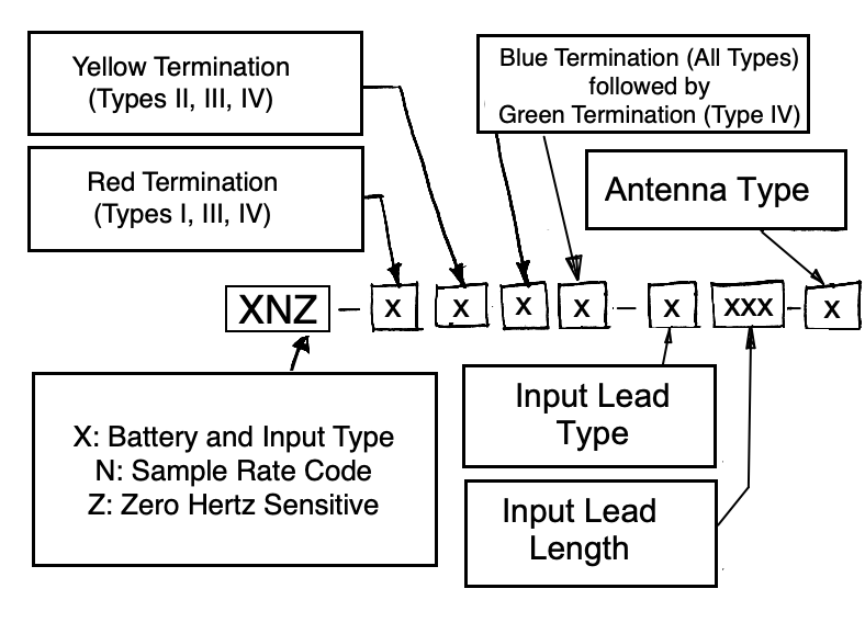
[05-JUN-26] The A3049 Subcutaneous Transmitter can be equipped with a dozen different sizes of battery and leads up to 280 mm long. It can be configured with one or two inputs, a dozen different lead terminations, several types of antenna, and a range of passbands, dynamic ranges, and sample rates. You specify which transmitter you want with a full SCT part number. The part number begins with A2049 and is followed by the primary version letter. This letter spceifies the battery and the input configuration. Following the primary version letter, we have the sample rate code. We use codes 1-5 for 128, 256, 512, 1014, and 2048 SPS respectively. We add the letter "Z" to indicate that the passband extends down to 0.0 Hz, making a "DC transmitter". We add an "S" to indicate that the battery should be mounted on the side of the circuit, making a "slim" transmitter, as opposed to the normal "thick" transmitters. Now comes a dash followed by letters indicating the terminations of the leads. After another dash comes a letter and a number specifying the type and length of the leads. After a final dash we have a letter specifying the antenna.
See our Electrode Catalog for a list of available lead terminations, and also for a presentation of the various depth electrodes to which these terminations can be attached. See our Leads Table for a description of our several types of insulated, coiled steel spring leads. See our Antennas table for a description of the various types of antenna we can deploy on our implants. The following versions are defined already, but we are happy to define new ones to suit your needs. The operating life is the minimum time for which a newly-made transmitter will operate continuously. The shelf life is the time the transmitter can remain in its lowest-power state on the shelf and still retain 90% of its operating life.
| Version | Input Config |
X Passband, Sample Rate, Dynamic Range |
Y Passband, Sample Rate, Dynamic Range |
Battery Capacity (μA·d) |
Volume (ml) |
Mass (g) |
Operating Life (d) |
Shelf Life (mo) |
|---|---|---|---|---|---|---|---|---|
| A3049W0Z | III | 0.0-20 Hz, 64 SPS, 120 mV | 0.0-20 Hz, 64 SPS, 120 mV | 1650 (CR1220) | 1.1 | 2.0 | 46 | 6 |
| A3049W2Z | III | 0.0-80 Hz, 256 SPS, 120 mV | 0.0-80 Hz, 256 SPS, 120 mV | 1650 (CR1220) | 1.1 | 2.0 | 21 | 0.1 |
| A3049A2S | III | 0.16-80 Hz, 256 SPS, 30 mV | 0.16-80 Hz, 256 SPS, 30 mV | 2000 (CR1225) | 1.3 | 2.3 | 24 | 7 |
| A3049A2Z | III | 0.0-80 Hz, 256 SPS, 120 mV | 0.0-80 Hz, 256 SPS, 120 mV | 2000 (CR1225) | 1.2 | 2.2 | 24 | 7 |
| A3049A3 | III | 0.16-160 Hz, 512 SPS, 30 mV | 0.16-160 Hz, 512 SPS, 30 mV | 2000 (CR1225) | 1.2 | 2.2 | 14 | 7 |
| A3049A3Z | III | 0.0-160 Hz, 512 SPS, 120 mV | 0.0-160 Hz, 512 SPS, 120 mV | 2000 (CR1225) | 1.2 | 2.2 | 14 | 7 |
| A3049A4 | III | 0.16-320 Hz, 1024 SPS, 30 mV | 0.16-320 Hz, 1024 SPS, 30 mV | 2000 (CR1225) | 1.2 | 2.2 | 7 | 7 |
| A3049B2 | I | 0.16-80 Hz, 256 SPS, 30 mV | Disabled | 2000 (CR1225) | 1.2 | 2.2 | 39 | 7 |
| A3049B3 | I | 0.16-160 Hz, 512 SPS, 30 mV | Disabled | 2000 (CR1225) | 1.2 | 2.2 | 25 | 7 |
| A3049B4 | I | 0.16-320 Hz, 1024 SPS, 30 mV | Disabled | 2000 (CR1225) | 1.2 | 2.2 | 14 | 7 |
| A3049J2 | IV | 0.16-80 Hz, 256 SPS, 30 mV | 0.16-80 Hz, 256 SPS, 30 mV | 2000 (CR1225) | 1.2 | 2.2 | 25 | 7 | <
| A3049J2Z | IV | 0.0-80 Hz, 256 SPS, 120 mV | 0.16-80 Hz, 256 SPS, 30 mV | 2000 (CR1225) | 1.2 | 2.2 | 25 | 7 | <
| A3049J2S | IV | 0.16-80 Hz, 256 SPS, 30 mV | 0.16-80 Hz, 256 SPS, 30 mV | 2000 (CR1225) | 1.3 | 2.3 | 25 | 7 |
| A3049J2ZS | IV | 0.0-80 Hz, 256 SPS, 120 mV | 0.16-80 Hz, 256 SPS, 30 mV | 2000 (CR1225) | 1.3 | 2.3 | 25 | 7 |
| A3049J3 | IV | 0.16-160 Hz, 512 SPS, 30 mV | 0.16-160 Hz, 512 SPS, 30 mV | 2000 (CR1225) | 1.2 | 2.2 | 14 | 7 |
| A3049J3ZS | IV | 0.0-160 Hz, 512 SPS, 120 mV | 0.16-160 Hz, 512 SPS, 30 mV | 2000 (CR1225) | 1.3 | 2.3 | 14 | 7 |
| A3049F2 | I | 0.16-80 Hz, 256 SPS, 30 mV | Disabled | 3300 (CR1620) | 1.4 | 2.9 | 65 | 10 |
| A3049F2S | I | 0.16-80 Hz, 256 SPS, 30 mV | Disabled | 3300 (CR1620) | 1.5 | 3.0 | 65 | 10 |
| A3049H2 | III | 0.16-80 Hz, 256 SPS, 30 mV | 0.16-80 Hz, 256 SPS, 30 mV | 3300 (CR1620) | 1.4 | 2.9 | 40 | 10 |
| A3049H2Z | III | 0.0-80 Hz, 256 SPS, 120 mV | 0.0-80 Hz, 256 SPS, 120 mV | 3300 (CR1620) | 1.4 | 2.9 | 40 | 10 |
| Version | Input Config |
X Passband, Sample Rate, Dynamic Range |
Y Passband, Sample Rate, Dynamic Range |
Battery Capacity (μA·d) |
Volume (ml) |
Mass (g) |
Operating Life (d) |
Shelf Life (mo) |
| A3049H3Z | III | 0.0-160 Hz, 512 SPS, 120 mV | 0.0-160 Hz, 512 SPS, 120 mV | 3300 (CR1620) | 1.4 | 2.9 | 23 | 10 |
| A3049K1 | IV | 0.16-40 Hz, 128 SPS, 30 mV | 0.16-80 Hz, 64 SPS, 30 mV | 3300 (CR1620) | 1.4 | 2.9 | 75 | 10 |
| A3049D2 | III | 0.16-80 Hz, 256 SPS, 30 mV | 0.16-80 Hz, 256 SPS, 30 mV | 11000 (CR2330) | 2.6 | 5.9 | 139 | 36 |
| A3049D3 | III | 0.16-160 Hz, 512 SPS, 30 mV | 0.16-160 Hz, 512 SPS, 30 mV | 11000 (CR2330) | 2.6 | 5.9 | 81 | 36 |
| A3049D3Z | III | 0.0-160 Hz, 512 SPS, 120 mV | 0.0-160 Hz, 512 SPS, 120 mV | 11000 (CR2330) | 2.6 | 5.9 | 81 | 36 |
| A3049D4 | III | 0.16-320 Hz, 1024 SPS, 30 mV | 0.16-320 Hz, 1024 SPS, 30 mV | 11000 (CR2330) | 2.6 | 5.9 | 43 | 36 |
| A3049E3 | I | 0.16-160 Hz, 512 SPS, 30 mV | Disabled | 11000 (CR2330) | 2.6 | 5.9 | 139 | 36 |
| A3049E3Z | I | 0.0-160 Hz, 512 SPS, 120 mV | Disabled | 11000 (CR2330) | 2.6 | 5.9 | 139 | 36 |
| A3049G2 | IV | 0.16-80 Hz, 256 SPS, 30 mV | 0.16-80 Hz, 256 SPS, 30 mV | 11000 (CR2330) | 2.6 | 5.9 | 139 | 36 |
| A3049M2 | III | 0.16-80 Hz, 256 SPS, 30 mV | 0.16-80 Hz, 256 SPS, 30 mV | 14000 (CR2050) | 3.0 | 6.5 | 180 | 48 |
| A3049N2 | IV | 0.16-80 Hz, 256 SPS, 30 mV | 0.16-80 Hz, 256 SPS, 30 mV | 14000 (CR2050) | 3.0 | 6.5 | 180 | 48 |
| A3049Q3 | III | 0.16-160 Hz, 512 SPS, 30 mV | 0.16-160 Hz, 512 SPS, 30 mV | 25000 (CR2450) | 4.0 | 8.7 | 184 | 82 |
| A3049Q3Z | III | 0.0-160 Hz, 512 SPS, 120 mV | 0.0-160 Hz, 512 SPS, 120 mV | 25000 (CR2450) | 4.0 | 8.9 | 184 | 82 |
| A3049Q4 | III | 0.16-320 Hz, 1024 SPS, 30 mV | 0.16-320 Hz, 1024 SPS, 30 mV | 25000 (CR2450) | 4.0 | 8.9 | 100 | 82 |
| A3049T5 | I | 0.16-640 Hz, 2048 SPS, 30 mV | Disabled | 25000 (CR2450) | 4.0 | 8.7 | 100 | 82 |
| A3049L4 | III | 0.16-320 Hz, 1024 SPS, 30 mV | 0.16-320 Hz, 1024 SPS, 30 mV | 42000 (CR2477) | 6.0 | 14.0 | 168 | 140 |
For each analog input we specify the bandwidth, sample rate, dynamic range, and channel number offset. In terms of ADC counts, the dynamic range is always 0-65535, as produced by the A3049's sixteen-bit ADC. The zero-value of an input is the sample we obtain when we short the two inputs together. The zero-value depends upon the battery voltage, VB, according to zero-value = 1.8 V · 65535 / VB. The dynamic range is the battery voltage divided by the gain of the amplifier. When we specify dynamic range, we assume VB = 3.0 V, which is true for almost the entire life of the lithium batteries we use with the A3049. When the amplifier gain is 100, the dynamic range is 30 mV and spans −18 mV to +12 mV.
See the Battery Life chapter of our telemetry manual for an explanation of how operating life of A3049-family devices varies with mass and sample rate. In almost all cases, we set the sample rate of an input equal to 3.2*B, where B is the bandwidth in Hz. This sample rate makes it possible for the low-pass filter to provide 20 dB attenuation at one half the sample rate, which is 1.6*B. Frequencies above one half the sample rate will be distorted by sampling, but the 20-dB attenuition ensures that such signals do not corrupt the signal we record from the SCT's passband.
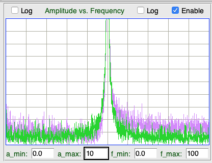
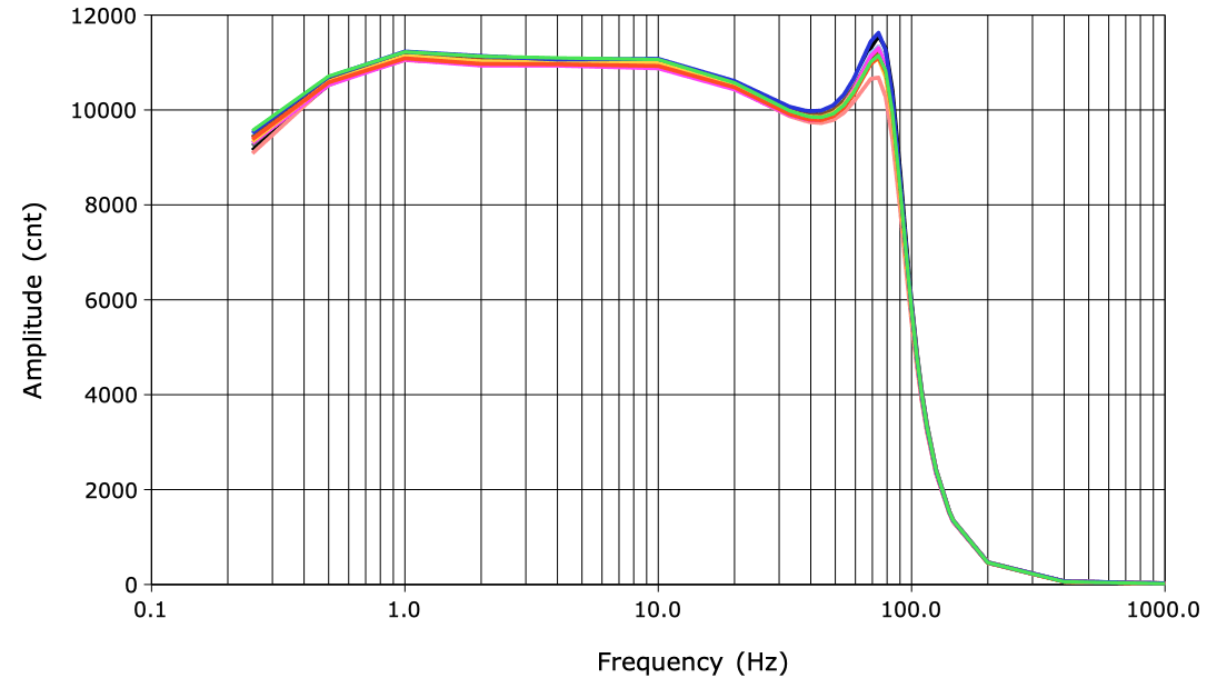
[18-JUN-25] The A3049 Subcutaneous Transmitter provides up to four signal inputs: X+, X−, Y+, and Y−. Each of these inputs has a reserved color for its leads: red, blue, yellow, and green respectively. These four leads are present or absent in accordance with each transmitter's input configuration. Whenever the X+ (red) lead is present, it uses the X− (blue) lead as its reference potential. When the Y+ (yellow) lead is present without the Y− (green) lead, the Y+ lead uses the X− lead as its reference potential. When the Y− lead is present, the Y+ uses the Y− lead as its reference potential. When equipped with three leads, the A3049 is a two-channel sensor with a shared reference potential. When equipped with four leads, it is a two-channel sensor with separate reference potentials. The figure below shows the frequency response of three A3049DZ3 after encapsulation. You will find a database of such plots here. We send one such plot along with each batch of transmitters we ship.
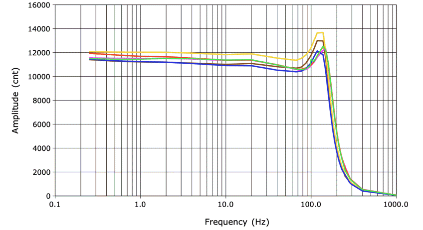
In the response shown above, we see the low-pass corner frequency marked by a bump in the gain just below the corner. If we define "corner frequency" as the frequency at which the gain drops to 70% of the gain in the passband, the corner frequency for this batch of transmitters is 180 Hz, which is slightly higher than the nominal 160 Hz we specify for the A3049D3Z. The most important function of the low-pass filter is to reduce the amplifier voltage gain by at least a factor of ten at a frequency that is one half the sample rate. We see that this is indeed the case for our batch of A3049D3Zs. They sample at 512 SPS and their gain at 256 Hz is less than 10% of their gain at 20 Hz.
| Range (mV) | Low (mV) | High (mV) |
|---|---|---|
| 30 | -18 | 12 |
| 60 | -36 | 24 |
| 120 | -72 | 48 |
| 150 | -90 | 60 |
| 300 | -180 | 120 |
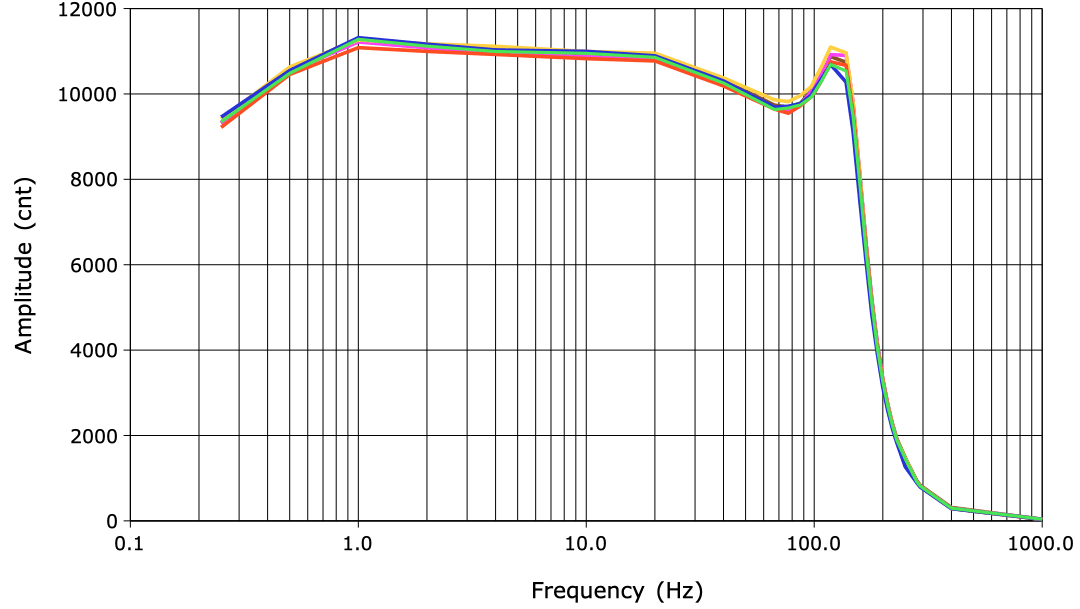
We specify for each analog input its absolute dynamic range, which is the difference between the high and low potentials at which the amplifier will saturate. The table above gives these high and low potentials for each standard A3049 Subcutaneous Transmitter input dynamic range. The figure below shows the frequency response of 0.16-160 Hz A3049AV3 prior to encapsulation. We can see the corner frequency of the high-pass filter. For a similar plot of 0.16-80 Hz A3049A2, see BV2_G_vs_G.gif.
The impedance of X input, as seen at the tips of its electrode leads, is 10 MΩ. When the Y input uses X− as its reference, the Y input impedance is 10 MΩ. When the Y input uses Y− as its reference, the Y input impedance is 20 MΩ. Most transmitters provide a high-pass filter by placing a capacitor in series with the input. The corner frequency of this high-pass filter is 0.2 Hz. When the input impedance is 10 MΩ, the high-pass filter presents a 100-nF capacitor in series with the input, and when the input impedance is 20 MΩ, the series capacitance is 50 nF. When we modify the transmitter to remove the high-pass filter, these capacitors will not be present at the input.
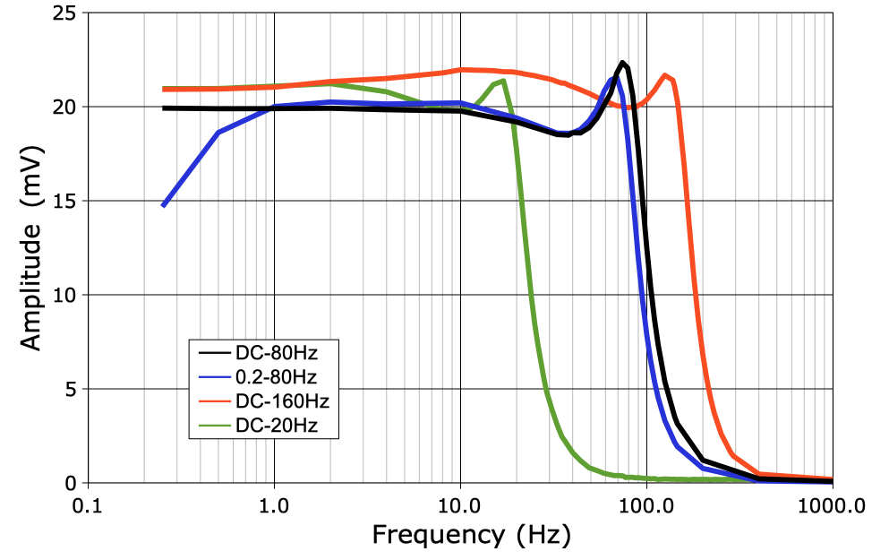
The X signal is supposed to measure the difference between X+ and X−. The average voltage of X+ and X− is the common mode voltage on X, and the difference between X+ and X− is the differential mode voltage. Suppose we apply the same sinusoidal voltage to both X+ and X−. The common mode voltage is the sinusoidal voltage and the differential mode voltage is zero. Under these circumstances, we would like X to be zero, but instead we will see a trace of the common-mode voltage appearing in the X signal. The ratio of the common-mode voltage amplitude and the X signal amplitude is the common mode rejection ratio, or CMRR. The plot below shows how the CMRR of X and Y vary with frequency.
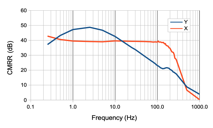
The X-input provides CMRR of 40 dB for frequencies below 160 Hz. The signal we see on X will be 1% the amplitude of the common-mode signal we apply to X. The CMRR of the Y-input is >40 dB for frequencies below 10 Hz, but drops for higher frequencies.
The distortion of a signal by an SCT is the extent to which the SCT changes the shape of the signal's sinusoidal components. We apply a 10 mVpp sinusoid to the X and Y inputs of an A3049A3, which provides passband 0.2-160 Hz and dynamic range 30 mV. We increase the frequency from 0.25 Hz to 200 Hz. For each frequency, we obtain the spectrum of the signal and measure the power outside the sinusoidal frequency as a fraction of the sinusoidal power using this script. We express the result in parts per million.
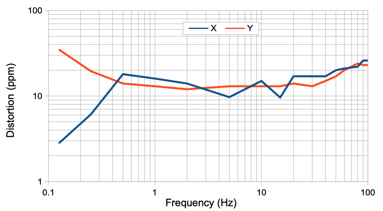
The distortion of the X is dominated by random electronic noise. There are no significant peaks in the spectrum outside the fundamental frequency of the sinusoidal input.
We note that the distortion generated by the A3049 Subcutaneous Transmitter is hundreds of time less powerful than that of its predecessor, the A3028. The A3049 samples the signal uniformly, thus eliminating the scatter noise present in the A3028 signal.
[18-JUN-25] We refer you to the Battery Voltage chapter of our Telemetry Manual for a discussion of how we can measure an A3049's battery voltage during operation.
[20-MAY-26] Our A3049 SCTs are equipped with non-rechargeable lithium coin cells. The operating life of an A3049 is how long it can amplify and transmit its input voltages when starting with a fresh battery. The shelf life of an A3049 is how long it can wait on the shelf in its sleep state before it has used 10% of its battery capacity. We specify minimum operating and shelf life in the A3049-family Version Table. We provide a detailed discussion of SCT operating life in the Battery Life chapter of our Telemetry Manual. Here we present tables and measurements specific to the A3049 Subcutaneous Transmitter family.
| Total Sample Rate (SPS) |
CR1216 1250 μA·d |
CR1225 2000 μA·d |
CR1620 3300 μA·d |
CR2025 6700 μA·d |
CR2330 11000 μA·d |
CR2450 22000 μA·d |
CR2477 42000 μA·d |
|---|---|---|---|---|---|---|---|
| 64 | 42 | 56 | 113 | 230 | 378 | 757 | 1445 |
| 128 | 34 | 45 | 90 | 185 | 304 | 609 | 1163 |
| 256 | 24 | 32 | 65 | 133 | 218 | 438 | 836 |
| 512 | 15 | 20 | 41 | 85 | 139 | 280 | 535 |
| 1024 | 8 | 11 | 24 | 49 | 81 | 162 | 311 |
| 2048 | 4 | 6 | 12 | 26 | 43 | 88 | 169 |
| 4096 | 2 | 2 | 6 | 13 | 22 | 46 | 88 |
The above table of operating life shows how sample rate and battery capacity dictate operating life. We calculated these operating life values using our worst-case quiescent and sampling current values, so the table gives the minimum operating life of a newly-made A3049 Subcutaneous Transmitter. The average operating life of the SCTS in our tests is roughly 10% longer.
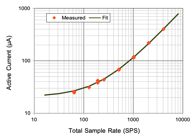
The active current consumption of A3049 Subcutaneous Transmitter increases linearly with sample rate, but also varies from one A3049 to another. For each version of the A3049, there is a maximum active current that we will accept during quality control. The minimum operating life of this version is its nominal battery capacity divided by its maximum active current. To see how we calculate the maximum active current of a particular A3049 version, see the Battery Life chapter of our Telemetry Manual.
[17-JUN-25] See the Implantation chapter of our Telemetry Manual for a presentation of implantation procedures and protocols. To record two EEG signals, we use a transmitter with input configuration III, in which the two signals share a common reference potential. We recommend connecting the blue lead to the cerabellum. The other two leads detect the potential somewhere else in the brain. To record EEG and EMG, we use a transmitter with input configuratin IV. We need each signal to be recorded with its own reference potential. The leads will be red and blue for EEG and yellow and green for EMG. We use blue as the ground potential of the implant, and connect to the cerabellum, which provides a good, stable mounting point. We secure the yellow and green leads to a muscle in the neck to record EMG.
[17-JUN-25] When we want to mark in our recordings the time at which some event took place, such as the start of a video recording or the moment at which we presented the host animals with a new visual stimulus, we can use an auxiliary SCT to add a synchronizing signal to our recording. See the Synchronization chapter of the Telemetry Manual for details.
[29-NOV-23] All versions of the A3049 Subcutaneous Transmitter are encapsulated in black epoxy and coated with silicone. The silicone is "unrestricted medical grade" MED-6607, meaning it is approved for implants of unlimited duration in any animal, humans included. The A3049's leads and antenna are encapsulated with dyed silicone, then coated with the same unrestricted medical grade silicone. The only materials the transmitter and its leads present to the subject animal's body are either unrestricted medical grade silicone or stainless steel. When we solder screws or pins to the ends of the leads, there is also solder. Solder reacts slowly with saline, so solder joints must be protected from body fluids by an insulating layer of cement during implantation.
[09-JUN-25] For design files and development logbook, see the A3049 Subcutaneous Transmitter design and development page at D3049.