In an attempt to automate part of the QC2 procedure for SCTs, we begin the design of a function generator that can be controlled through an RJ-45 socket with LWDAQ. We begin by looking at the design done by Michael Bradshaw (A3031). With our new design, we plan to use a similar method to change frequency output but allow the device to be controllable over a socket without a LWDAQ driver involved. This instrument will allow us to perform a frequency sweep on our circuits and measure the response in a LWDAQ instrument. We begin with the same RCM6700 module and logic as the ALT baseboards. This will provide communication over the socket. The logic will then transmit a signal through two identical channels, starting with an 8-bit DAC. This will output a rough sinusoid that can then be smoothed out with an RC circuit. We switch to different RC circuits depending on the update rate of the signal using DG411Y chips. We include power LEDs and indicator lights to make testing the board easier.
The first version of the PCB did not route the feedback of the op-amps correctly, and as a result the op-amps consumed too much current. We also forgot to include a programming extension for the logic chip and as a result we had to solder some wires to individual pins. We also plan to replace the 80MHz clock currently on the board with one that has a bigger footprint. The board has plenty of space and it will be easier to solder and test.
| Control Space Address (Hex) | Contents |
|---|---|
| 00 | Hardware identifier |
| 12 | Hardware version |
| 13 | Software version |
| 18 | Data address 1 |
| 19 | Data address 2 |
| 1A | Data address 3 |
| 1B | Data address 4 |
| 3F | Data portal |
All of the registers necessary for controlling the function generator are located in the data space.
| Data Address (Hex) | Contents |
|---|---|
| 0000...1FFF | Sample values, Channel 1 |
| 4000...5FFF | Sample values, Channel 2 |
| 8000 | RC filter switch controller, Channel 1 |
| 8001 | RC filter switch controller, Channel 2 |
| 8002 | Divisor, Channel 1, Byte 3 |
| 8003 | Divisor, Channel 1, Byte 2 |
| 8004 | Divisor, Channel 1, Byte 1 |
| 8005 | Divisor, Channel 1, Byte 0 |
| 8006 | Divisor, Channel 2, Byte 3 |
| 8007 | Divisor, Channel 2, Byte 2 |
| 8008 | Divisor, Channel 2, Byte 1 |
| 8009 | Divisor, Channel 2, Byte 0 |
| 800A | Waveform length, Channel 1, Byte 1 |
| 800B | Waveform length, Channel 1, Byte 0 |
| 800C | Waveform length, Channel 2 Byte 1 |
| 800D | Waveform length, Channel 2 Byte 0 |
| 800E | Attenuation for both channels |
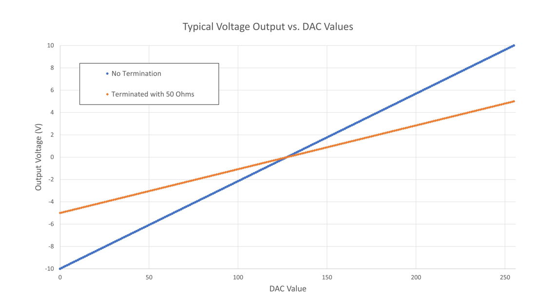
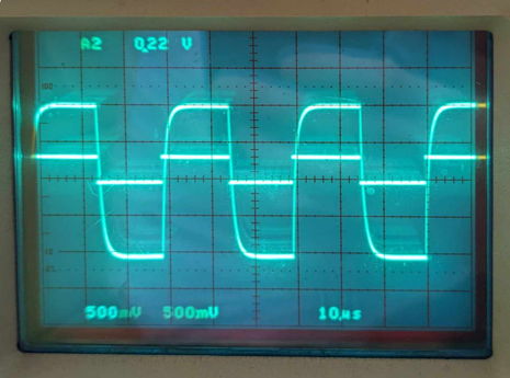
As an example, we will generate a 5V 100kHz square wave with an offset. We begin by writing [128, 255 (dec)] to the first two locations in the data space. The full range of DAC values is 0 to 255 (dec) so if we change between 128 and 255 the waveform will be offset by 5V and have a ptp amplitude of 10V. We then set the waveform length to 2 by writing [0, 1 (dec)] to 800A. Lastly, we write [0, 0, 0, 199 (dec)] to location 8002. This determines the divisor for the clock that sets the speed at which the function generator is reading from RAM. Below is an equation for determining the frequency of the output waveform.

We use some variables to make the equations look neat. We define "waveform frequency" as the frequency of the sine wave, square wave, or arbitrary waveform that is generated on the output of the function generator. We define "sample frequency" as the rate at which the function generator reads from the RAM, moving onto the next sample value. We define "waveform length" as a unitless variable equal to the number of samples required to complete one cycle of the output waveform. Lastly, we define "clock divisor" as the value we provide in order to change the sample rate. We provide a plot of output voltage versus DAC value below such that anyone operating the function generator can generate any voltage within the acceptable range. For this example waveform, we do not need to write to the RC filter registers because the default RC filter is the smallest time constant possible which gives us the sharpest square wave possible. Different possible time constants the function generator can use are in the table below:
| Binary | Hex | Decimal | Resistance | Capacitance | Time Constant |
|---|---|---|---|---|---|
| 00000001 | 01 | 01 | 51 Ω | 250 pF (parasitic) | 12.5 ns |
| 00010001 | 11 | 17 | 51 Ω | 1 nF | 51 ns |
| 00010010 | 12 | 18 | 110 Ω | 1 nF | 110 ns |
| 00010100 | 14 | 20 | 270 Ω | 1 nF | 270 ns |
| 00011000 | 18 | 24 | 560 Ω | 1 nF | 560 ns |
| 00100001 | 21 | 33 | 51 Ω | 22 nF | 1.12 μs |
| 00100010 | 22 | 34 | 110 Ω | 22 nF | 2.42 μs |
| 00100100 | 24 | 36 | 270 Ω | 22 nF | 5.94 μs |
| 00101000 | 28 | 40 | 560 Ω | 22 nF | 12.3 μs |
| 01000001 | 41 | 65 | 51 Ω | 500 nF | 25.5 μs |
| 01000010 | 42 | 66 | 110 Ω | 500 nF | 55 μs |
| 01000100 | 44 | 68 | 270 Ω | 500 nF | 135 μs |
| 01001000 | 48 | 72 | 560 Ω | 500 nF | 280 μs |
| 10000001 | 81 | 129 | 51 Ω | 20 μF | 1.02 ms |
| 10000010 | 82 | 130 | 110 Ω | 20 μF | 2.2 ms |
| 10000100 | 84 | 132 | 270 Ω | 20 μF | 5.4 ms |
| 10001000 | 88 | 136 | 560 Ω | 20 μF | 11.2 ms |
The two data address locations that control the RC filters for both channels use 1 byte to control all 8 switches within one channel. The diagram below shows us an example of all the switches being open with the exception of 100 Ω. For more info on how LWDAQ messages are used to communicate with the control space, see LWDAQ Specification. For an example of using control space to create a data space through a data portal, see LWDAQ Driver Manual.
| Channel Number | Data Address (Hex) | Bit of 8-Bit Register | Passive Component Being Switched |
|---|---|---|---|
| 1 | 8000 | 0 | 51R |
| 1 | 8000 | 1 | 110R |
| 1 | 8000 | 2 | 270R |
| 1 | 8000 | 3 | 560R |
| 1 | 8000 | 4 | 1nF |
| 1 | 8000 | 5 | 22nF |
| 1 | 8000 | 6 | 500nF |
| 1 | 8000 | 7 | 20μ |
| 2 | 8001 | 0 | 51R |
| 2 | 8001 | 1 | 110R |
| 2 | 8001 | 2 | 270R |
| 2 | 8001 | 3 | 560R |
| 2 | 8001 | 4 | 1nF |
| 2 | 8001 | 5 | 22nF |
| 2 | 8001 | 6 | 500nF |
| 2 | 8001 | 7 | 20μ |
Here we use the default 12.5ns time constant which can be set by resetting the function generator or by writing 01 to the location 8000 (Hex) to the data space. We also choose to not attenuate the signal at all so we do not have to write to that register seeing as the default is no attenuation. If we were to attenuate the signal we could use the table below to choose by how much the signal would be attnuated:
| Channel Number | Data Address (Hex) | Bit of 8-Bit Register | Attenuator Being Selected |
|---|---|---|---|
| 1 | 800E | 0 | -3dB |
| 1 | 800E | 3 | -4.8dB |
| 1 | 800E | 2 | -7dB |
| 1 | 800E | 1 | -9.6dB |
| 2 | 800E | 4 | -3dB |
| 2 | 800E | 7 | -4.8dB |
| 2 | 800E | 6 | -7dB |
| 2 | 800E | 5 | -9.6dB |
The resulting waveform is below:

The function generator's registers always reset to the same values, see table below:
| Parameter | Reset Value (Dec) |
|---|---|
| Sample Values, Channel 1 | 128 (Output = 0V) |
| Sample Values, Channel 2 | 128 (Output = 0V) |
| RC filter switch controller, Channel 1 | 1 |
| RC filter switch controller, Channel 2 | 1 |
| Divisor, Channel 1, Bytes 0-3 | All 0 |
| Divisor, Channel 2, Bytes 0-3 | All 0 |
| Waveform Length, Channel 1, Bytes 0-1 | All 0 |
| Waveform Length, Channel 2, Bytes 0-1 | All 0 |
| Attenuation switch controller, both channels | All 0 |
The waveform generated has a maximum amplitude of +/- 10V but if the channel is terminated with 50 ohms then the maximum amplitude of the waveform becomes +/- 5V. This function generator is designed to provide proper transmission down a 50-ohm coaxial cable terminated with a 50-ohm resistor.
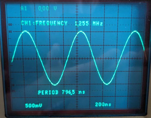
Next, we will generate a 10V 1.25MHz sine wave. We begin by writing the values [128, 152, 176, 198, 218, 234, 245, 253, 255, 253, 245, 234, 218, 198, 176, 152, 128, 103, 79, 57, 37, 21, 10, 2, 0, 2, 10, 21, 37, 57, 79, 103 (dec)] to the first 32 locations in the data space. Lastly, we write [0, 31 (dec)] to address 800A. This changes the waveform length to allow for the first 32 DAC values to be read out repeatedly. Notice that writing 31 as the waveform length allows for a waveform of 32 samples. The actual waveform length will be one more than the value written to the register. We do not change the divisor because we wish to generate 1.25MHz which is achieved with no divisor and a waveform length of 31. The resulting waveform is below:
Finally, we will generate a smoothed 10V 10kHz sine wave. The 1.25 MHz sine wave was fast enough that it didn't require a base load capacitor to smooth out. Something slower will have noticeable steps if not smoothed. We begin by writing the same DAC sine wave values as the first waveform [128, 152, 176, 198, 218, 234, 245, 253, 255, 253, 245, 234, 218, 198, 176, 152, 128, 103, 79, 57, 37, 21, 10, 2, 0, 2, 10, 21, 37, 57, 79, 103 (dec)] to the first 32 locations in the data space. We then write [0, 31 (dec)] to address 800A to guarentee the waveform reads all 32 DAC values and only those 32 DAC values. We also write [0, 0, 0, 124 (dec)] to location 8002 in order to change the waveform's frequency by a factor of 125. If we write [1 (dec)] to address 8000 then the output will look something like this:
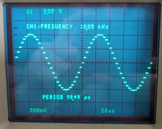
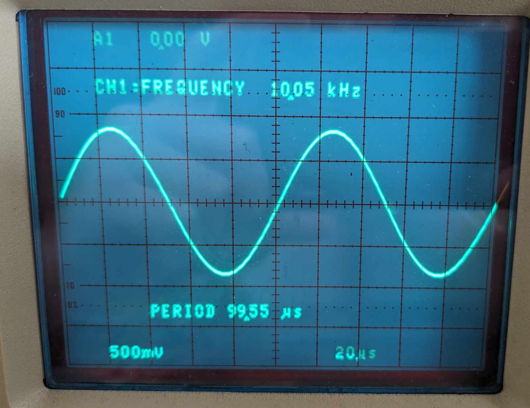
Notice how we can see each sample as a step rigidly separated from the others. To avoid this, we can write [34 (dec)] to location 8000 which gives us a 10us RC filter. The resulting waveform has about 13% less amplitude but looks much smoother:
We want to design the function generator such that it can output frequencies from a few megahertz to less than one hertz. To accomplish the faster frequencies we load an 80MHz clock onto the board going directly to logic. This clock signal is then divided by an amount determined by a register and then used as the trigger for when to read from RAM. This way we can slow the clock down by dividing its frequency by some integer. The LCMXO2-7000HC then reads the RAM values and writes them to the 8-bit DAC we load on the logic output with 0.1 percent precision resistors which gives us a waveform with steps in it. Each step represents reading a new RAM value. This rigid waveform however does not have an average value of zero volts because the logic outputs a DAC voltage between 0V and 3V3. To set the average value to zero we tie the DAC output to the non-inverting input 3V3 to the inverting output through a 1k resistor. Since the DAC output should be centered around 1V65 we use a feedback resistor of 1k causing the signal on the output to have a gain of 2 and be offset by 1V65. We then run the signal through two analog switches that allow the user to select which RC filter they would like to use to smooth out the jagged waveform. The filtered waveform is then passed through another amplifier with a gain of 3 and no offset. Afterwards the output of this amplifier is connected to a 2k resistor followed by an analog switch which controls which resistors are connecting the signal to ground. Using this method we can attenuate a signal using control lines from our logic chip. Lastly, the signal is put through an amplifier with a gain of 1 that acts as a buffer which can supply the current necessary for the final waveform. This signal is then put through a 50R 3W resistor and goes out to a BNC connector. We repeat this method using different I/O pins on the logic to create a second signal output. Now we can use this function generator to output an arbitrary waveform of any frequency between less than 1 Hz and 5MHz with an amplitude of +/- 10V.
[20-OCT-23] Create manual page.
[25-OCT-23] We receive new PCBs (A305001B) and assemble one. We notice that as soon as power is supplied, the +/-12V DC-DC converter begins buzzing. The logic chip can program so we now have a working extension, but we found that we must remove the feedback capacitors (10pf) on each op-amp in order to avoid drawing too much current. After removing these capacitors, we put a 3.3V 32.768kHz signal through both DAC channels and watch it propagate through the amplifiers. Each channel outputs a 10Vptp 32.768kHz signal with a 0V average.
[18-DEC-23] We program the controller (LCMXO2-7000HC) with a relay interface that maps various address spaces to variables needed to output a function. The data portal is located in the highest location in the control space.
[24-JAN-24] To avoid supply shortage issues later on, we develop a DC-DC converter using the LT8306 no-opto isolated flyback converter. Using the LT8306 datasheet, we come to the following design:
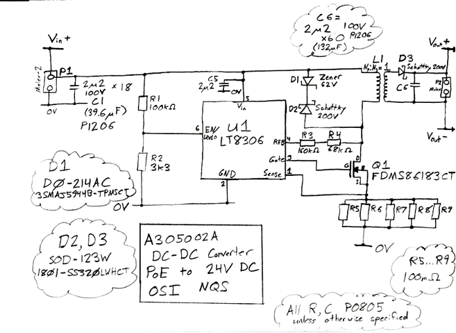
Once assembled, we test the converter by slowly ramping up its input voltage with a DC benchtop power supply and measuring its current consumption as well as its output voltage.
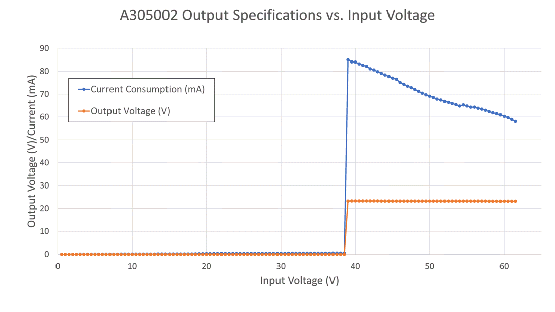
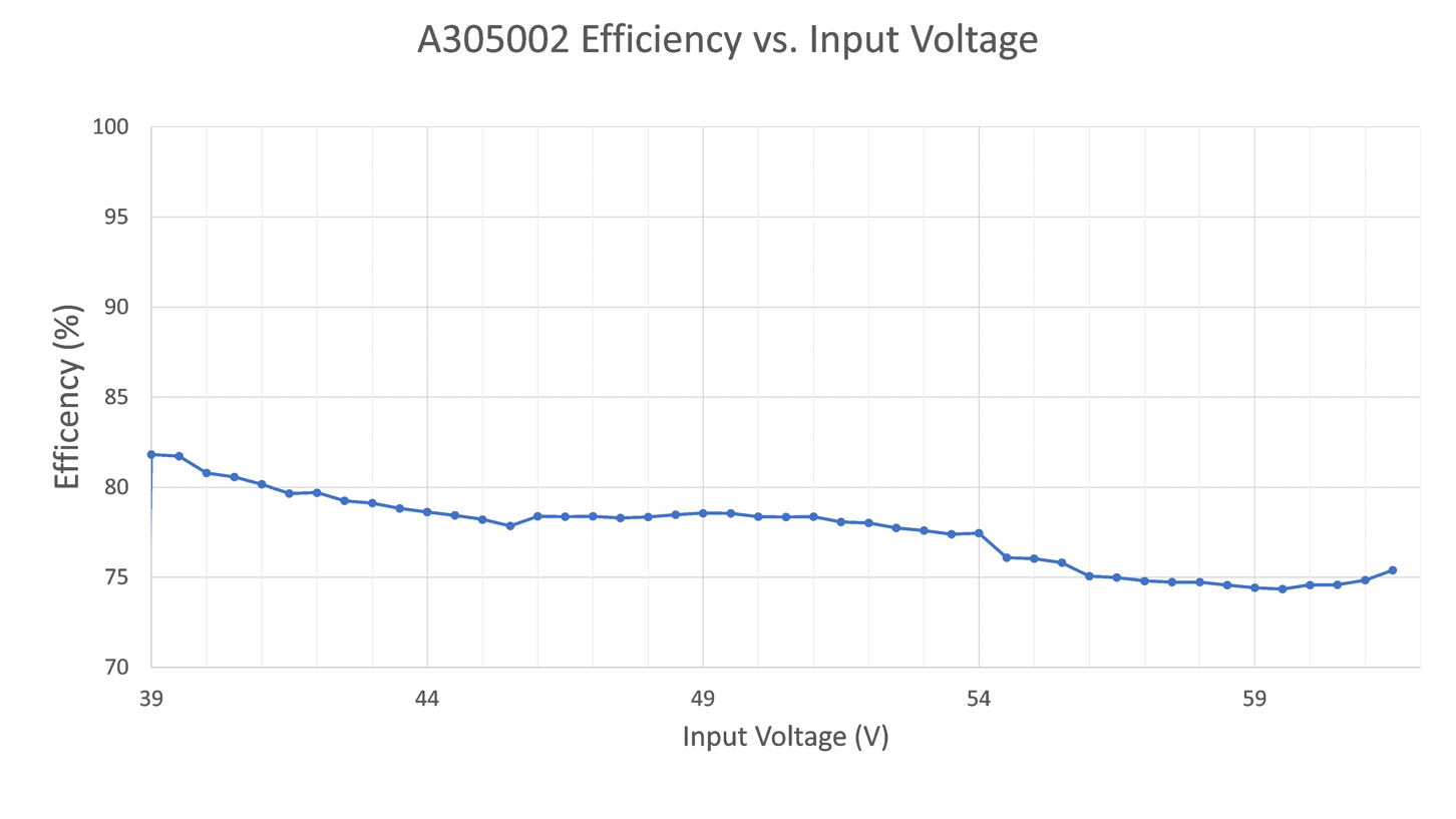
We then use these measured values to calculate the input power and output power. The effieciency measured in the graph below is defined as the output power divided by the input power.
[29-JAN-24] We notice that with a 0.01 Ohm sense resistor the output voltage varies greatly based on input voltage. We increase the sense resistor to 0.025 Ohms and notice that the output voltage stabalizes with respect to input voltage.
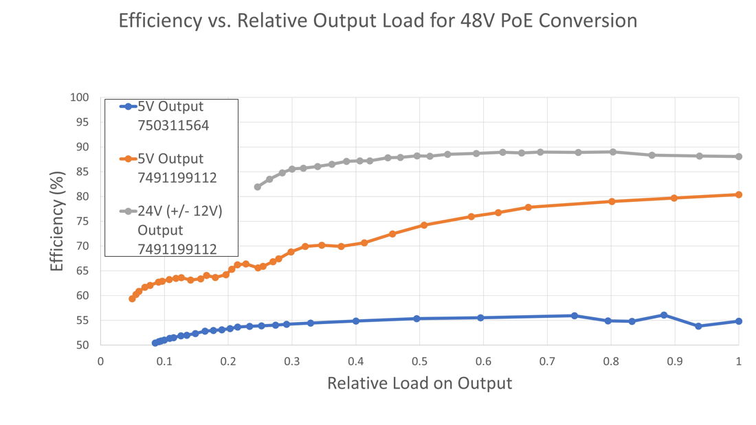
[07-MAY-24] We change the transformer used and attempt to output different voltages, measuring efficiency while increasing the output power.
[17-APR-24] We get a new PCB for the DC-DC converter, A305002B and test. This new PCB allows us to choose between one output voltage and two differential output voltages by loading 0R resistors on some P0805 footprints. This allows us to use one PCB for different converters, versions below:
| Version | R6 Value | R7 Value | R8 Value | Output Voltage |
|---|---|---|---|---|
| A3050DC-S5 | OC | SC | SC | +5V |
| A3050DC-D5 | SC | OC | OC | ±5V |
| A3050DC-S12 | OC | SC | SC | +12V |
| A3050DC-D12 | SC | OC | OC | ±12V |
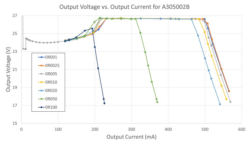
[17-APR-24] We assemble a converter in the ±12V configuration and plot its output voltage vs its output current for various values of R_sense. Results below:
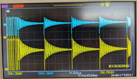
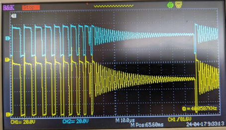
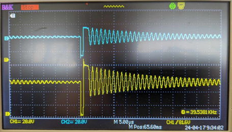
[18-APR-24] We measure the voltage at the drain of the MOSFET and the output of the transformer using an oscilloscope at various time divisions. Plots below.