| Description |
| Versions |
| Operation |
| Antennas |
| Digital Input-Output |
| Firmware Versions |
| Firmware Reprogramming |
| Indicator Lamps |
| Design |
Retirement Notice: The A3027 Octal Data Receiver is no longer in production. It has been replaced by the Telemetry Control Box (TCB, or A3042).
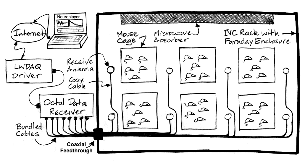
[20-MAR-26] The A3027 Octal Data Receiver (ODR) is a coaxial-antenna data receiver for use with our Telemetry System. The A3027 provides eight independent antenna inputs to which we can connect up to sixteen Telemetry Antennas (A3015). We connect these antennas using 50-Ω coaxial cables terminated with BNC plugs. These antennas pick up the signals transmitted by our wireless telemetry sensors and carry them to the radio receiver circuits in the A3027. The A3027 also provides four general-purpose digital signals on the front panel that we can configure for particular experiments.
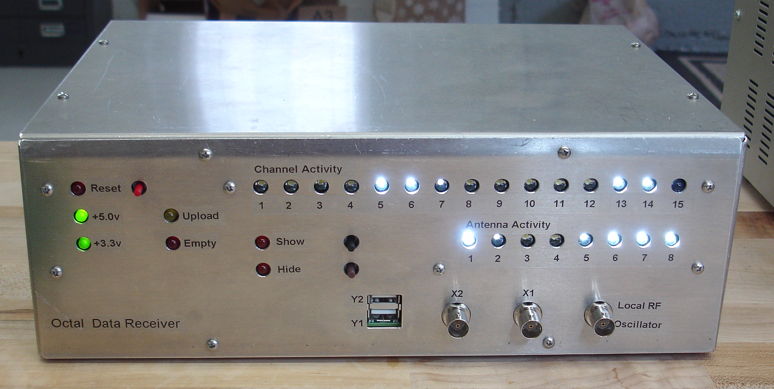
The A3027 Octal Data Receiver provides thirty indicator lamps. The top row of fifteen lamps shows us transmitter activity. Activity on any channel number with remainder one (1) when divided by sixteen (16) will contribute to the brightness of the channel one (1) activity light. The channel seven (7) activity light is for channel numbers with remainder seven (7) when divided by sixteen (16). The fifteenth channel activity light is blue, for the auxiliary channels, which are those with remainder fifteen (15). The bottom row of eight LEDs tell us the activity on each of the eight antenna inputs. The two green lights indicate power is on. The yellow light is UPLOAD to the LWDAQ Driver. The red light is EMPTY message buffer. These two lights shine together when the LWDAQ is reading out messages as they are received by the A3027. The red switch is hardware RESET. The red light beside it is the RESET indicator. The brown and black switches, with their neighboring orange lamps, are the display function switches, SHOW and HIDE. When we press SHOW, all activity lights turn on. When we press HIDE, the activity lights toggle between being disabled and enabled. We disable the lights to reduce the current consumption of the A3027, which permits us to connect two A3027s to one LWDAQ Driver (A2071E).
With its eight independent radio-frequency receivers, the A3027 Octal Data Receiver will often pick up multiple copies of each telemetry message transmitted by the sensors in one of our Faraday enclosures. The A3027 eliminates almost all such duplicates before it stores them to its message buffer. Some duplicates remain, but these are eliminated by the Receiver Instrument as soon as it receives the data from the A3027.
The following A3027 Octal Data Receiver versions exist. For each, we give the minimum firmware version used to program the circuit's logic chips. The firmware version is available in the last byte of every clock message retrieved from the A3027, as it is with the older A3018. In order to distinguish the Octal Data Receiver (A3027) from the earlier Data Receiver (A3018), we add 30 to the A3027 firmware version to create the number in the final byte of the clock message. When the A3027 firmware version is 4, the last byte of the clock message will be 34. You can determine the firmware version of your A3027 by setting show_messages to 1 in the Neurplayer's configuration panel. When you play back an interval, the firmware version number will be printed.
| Assembly Version |
Description | |
|---|---|---|
| A | First prototype, no display board, no enclosure. | 2 |
| B | Second prototype, hand-written labels. | 3 |
| C | First production version, with hide and show buttons, printed labels. | 4+ |
| D | Increased demodulator gain, otherwise as A3027C. | 4+ |
| E | Stabilized intermediate frequency amplifier, dramatic performance improvement. | 4+ |
We describe the firmware versions below. Starting with firmware version nine (9), the A3027 supports communication with Animal Location Trackers (A3032). Starting with firmware version ten (11), the A3027 supports channel numbers 1-222 rather than the original 1-14. The Set Select Register on the A3027 permits the Receiver Instrument to configure the A3027 to record from only one transmitter set or from all of them.
[08-NOV-25] The A3027 Octal Data Receiver is a LWDAQ Device. We plug it into a LWDAQ Driver with a LWDAQ Cable. We connect the LWDAQ Driver to a local wired Ethernet with an Ethernet jumper cable. Now we can communicate with and read out the A3027 over the wired network through the LWDAQ Driver. The cable we use to connect the A3027 to the LWDAQ Driver is also a network cable, and it plugs into the RJ-45 socket on the back of the A3027, and then into one of the RJ-45 sockets on the front of the LWDAQ Driver. Note that these RJ-45 sockets are not for Ethernet, but for LWDAQ communication and power delivery.
When instructed to do so by the Receiver Instrument in our LWDAQ Software, the LWDAQ Driver sends sixteen-bit commands to the A3027, and downloads data from the A3027 data buffer. The following table gives the A3027's allocation of the sixteen command bits.
| DC16 | DC15 | DC14 | DC13 | DC12 | DC11 | DC10 | DC9 | DC8 | DC7 | DC6 | DC5 | DC4 | DC3 | DC2 | DC1 |
|---|---|---|---|---|---|---|---|---|---|---|---|---|---|---|---|
| R7 | R6 | R5 | R4 | R3 | R2 | R1 | R0 | WAKE | LB | X | DTX | X | X | ISTS | RESET |
The WAKE bit is reserved for LWDAQ, but serves no function on the A3027. The LB (loop-back) bit sets up the A3027's LWDAQ interface for a measurement of the total propagation delay from the driver to the A3027 and back again. We use the loop-back function when looking for problems with the LWDAQ communication. The DTX (data transmit) bit directs the A3027 to transmit the next byte from its data buffer when it receives a falling edge on the logic signal from the driver. The RESET bit resets the storage and readout memory addresses and many other internal state machines. It's the bit we write to from the Receiver Instrument to reset the data receiver. The ISTS (instant sample transmission select) bit is available in most, but not all, firmware versions. When we set ISTS, the upper bits R0..R7 represent a seven-bit channel number that the A3027 will match for immediate sample transmission on one of the general-purpose digital outputs.
[08-NOV-25] The A3027 provides eight independent antenna inputs so as to permit robust reception from moving subcutaneous transmitters. In order for the antennas to be independent in their reception of radio-frequency waves, we must place them at least 30 cm apart, which is one wavelength of 915 MHz in air. When we arrange antennas in a Faraday enclosure, we should make sure they are at least 5 cm from the conducting walls of the enclosure as well as separated by at least 30 cm. If the antennas are too close to the conducting walls, they stop working. If they are too close to one another, they do not provide the independent reception that permits us to increase overall reception from many animals to ≥98%. The figure below is an example of an effective antenna arrangement.
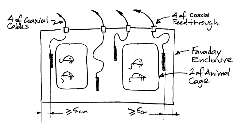
We can increase the operating area of our recording system further by connecting two antennas to each A3027 antenna input using a BNC T-junction. Two antennas connected to the same antenna input provide additional operating range provided the two antennas are in separate Faraday enclosures, or they are least 60 cm apart within the same Faraday enclosure.
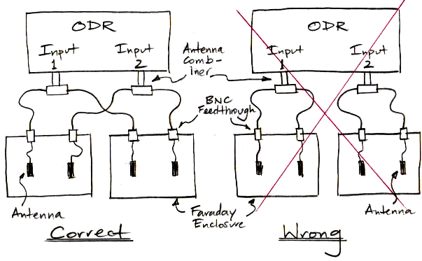
Transmitter messages are received correctly when their power is more than ten times the power of the ambient radio-frequency interference in the 902-928 MHz band. Otherwise, the interference dominates. With eight independent antennas, the A3027 provides multiple opportunities for a transmitter message to be received and decoded. If we have four antennas in each of four bench-top Faraday enclosures and we connect them in pairs to the eight A3027, we have four independent antennas in each enclosure with which to receive telemetry signals. So long as the radio-frequency power of a telemetry message is ten time interference power at one or more of these four nearby antennas, the message will be received.
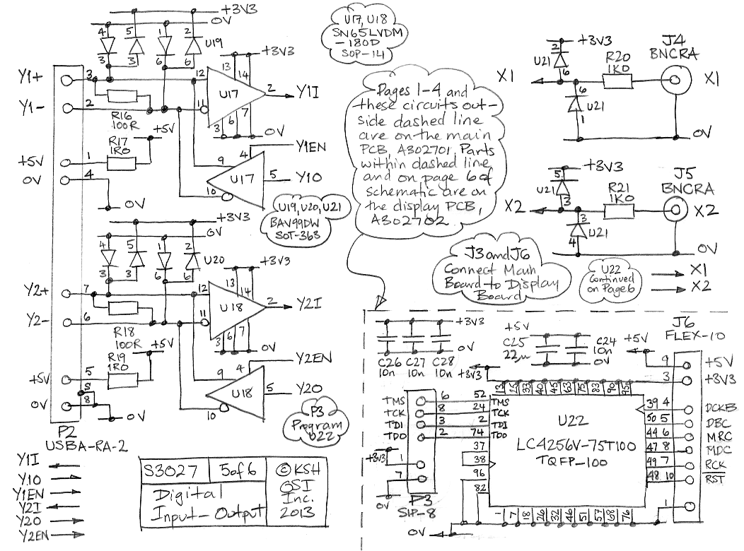
[02-APR-16] The A3027 provides two bi-directional low-voltage differential logic signals (LVDS) and two bi-directional 3.3-V single-ended logic signals. The S3027_5 schematic shows all four logic signals and their connectors. The LVDS signals are Y1 and Y2. They are available on the front panel of the A3027 on two USBA plugs. These plugs also provide 5-V power for auxiliary circuits. The single-ended signals are X1 and X2. They are available on the front panel on two BNC sockets. There is a 1-kΩ resistor in series with X1 and X2, and diode clamps, to protect the A3027 logic chips from electrostatic discharge and external over-voltages. The A3027 firmware determines the behavior of each signal. We describe the behavior of the inputs and outputs in below.
[28-JUN-25] The A3027 firmware version determines the behavior of the inputs and outputs, as well as correcting bugs in the operation of the logic, and adding features such as increasing the range of channel numbers from 0-15 to 0-255. Look in the Receiver Instrument or Neurorecorder Tool for notification of your A3027 firmware version. If you have a firmware version V11 or lower, we recommend you arrange for a firmware update. If you have firmare version V12, read the section below on V12 for an explanation of odd behavior of the activity lights. To re-program your firwmare, see Firmware Reprogramming. For an example of a program that uses the A3027 logic outputs to control other hardware, consider the Slow Pulse Generator.
| Firmware | X1 | X2 | Y1 | Y2 | Features |
|---|---|---|---|---|---|
| 4 | Antenna One Detecting | Unused Input | Message Detector Code | Unused Input | None |
| 5 | Antenna One Detecting | Immediate Sample Transmission | Message Detector Code | Unused Input | None |
| 6 | User Logic Output | User Logic Output | Message Detector Code | Immediate Sample Transmission | None |
| 7 | User-Enabled Pulses, 1 ms at 24.6 Hz. | User Logic Output | Message Detector Code | Immediate Sample Transmission | None |
| 8 | User Logic Output | Immediate Sample Transmission | Prototype Message Notification | Prototype Message Notification | None |
| 9 | User Logic Output | Immediate Sample Transmission | Message Notificaion for Location Trackers | Message Notification for Location Trackers | None |
| 10 | User Logic Output | Immediate Sample Transmission | Message Notificaion for Location Trackers | Message Notification for Location Trackers | Support for SCT set numbers, default Set 0, no duplicate rejection. |
| 11 | User Logic Output | Immediate Sample Transmission | Message Notificaion for Location Trackers | Message Notification for Location Trackers | Support for SCT channels 1-254, default Set 0, no duplicate rejection. |
| 12 | User Logic Output | Immediate Sample Transmission | Message Notificaion for Location Trackers | Message Notification for Location Trackers | Support for SCT channels 1-245, default Set 0, with duplicate rejection. |
| 13 | User Logic Output | Immediate Sample Transmission | Message Notificaion for Location Trackers | Message Notification for Location Trackers | Support for SCT channels 1-245, default all sets, duplicate rejection. |
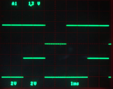
Firmware V4: The X1 output is Antenna One Detecting. Any time Antenna One receives something that starts to look like an SCT message, X1 goes HI. The photograph below shows X1 when we are receiving perfectly from three transmitters that are not colliding.
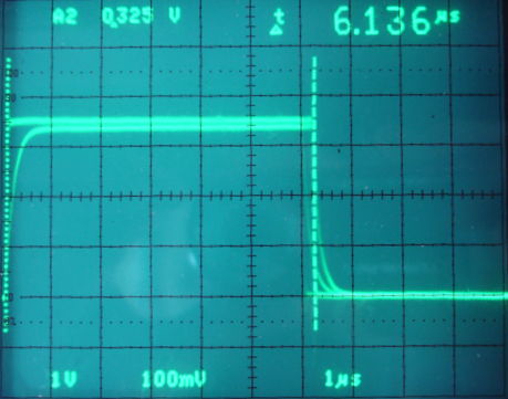
We use the X1 signal to trigger on SCT transmissions so we can examine signals inside the A3027 and watch the transmit bits as they are amplified and demodulated. The X1 signal is asserted after five synchronizing edges are received from the transmitter. The 6.1 μs detection time is the remaining 31 bits transmitted by these SCTs, at a nominal 200 ns per bit, gives 6.2 μs. The actual bit time varies from one transmitter to the next, which is why there are three falling edge locations in the photograph.
Firmware V5: We configure the A3027 for Immediate Sample Transmission. By transmitting a command through the LWDAQ to the A3027 we select one channel number for immediate transmission as a sixteen-bit serial word on X2. A LWDAQ command is itself a sixteen-bit number. We can send individual commands to the A3027 with the Diagnostic Instrument. The sixteen-bit hexadecimal command 0n02 instructs the A3027 to transmit all samples it receives from channel number n. When the A3027 powers up, the selected channel number is zero, so the A3027 transmits the samples of channel zero, which is the timestamp channel. The transmitted samples start at zero and increase to 65535 at 128 SPS. If we turn on an A3028A dual-channel 512 SPS transmitter using channels 1 and 2, we can select the first channel for immediate transmission with command 0102. If we want to select channel number 141, we must translate 141 into hexadecimal, and enter 8D02. The channel selection will remain in place until we send another command to change its value, or we press the front-panel hardware reset button, or we cycle the power.
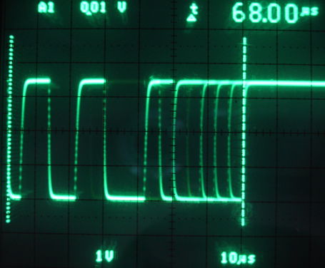
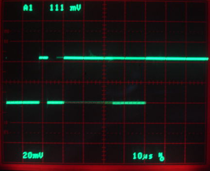
The speed with which we can transmit the sixteen-bit serial word is limited by the length of the coaxial cable we use to carry the signal to our external logic, and the terminating capacitance at the end of the cable. The photograph below shows a 333 kHz clock on X2 with a 2.6-m RG58C cable and a 50-pF terminating capacitor.

The flickering in the rising and falling edges are periodic steps in the edges with period 28 ns. Our coaxial cable has propagation delay 4.0 ns/ft and length 2.6 m. The signal takes 10.4 ns to reach the far end of the cable, where it is reflected, and 10.4 ns to come back. When we shorten the cable to 107 cm, the period of the steps drops to 11 ns. The immediate sample transmission proceeds at 4 μs per bit, so as to give plenty of time for the signal at the other end of a 2.6-m cable to settle for each bit. The photograph below shows the transmission of timestamp samples.
The X2 output has a rest state of 3.3 V, or logic HI. To initiate serial transmission, it asserts a 0.0 V, or logic LO, for one 4-μs bit period. It proceeds from there to transmit the sample bits one at at time, from the most significant to the least significant.
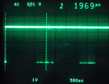
If we expand the oscilloscope view, we start to see subsequent samples. The photograph above shows the subsequent sample transmissions when we select a 512 SPS transmitter. Transmitters have sample scatter, as we describe elsewhere. Thus the samples do not arrive at a uniform rate, but rather at an average rate of 512 SPS.
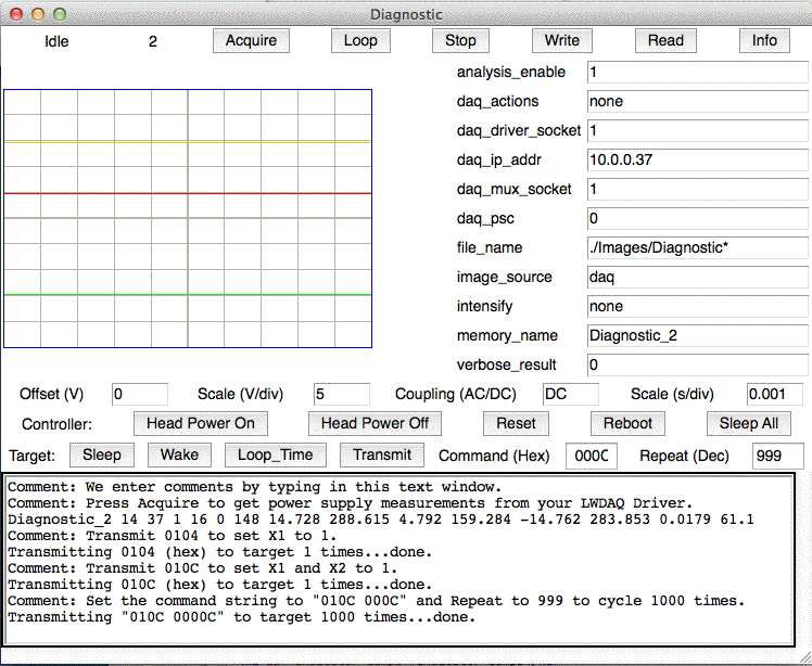
Firmware V6: We configure X1 and X2 to be digital outputs set by LWDAQ Commands. The Immediate Sample Transmission of V5 now goes to Y2 and the Antenna One receiving signal goes to Y1. To set X1 to 1, or 3.3 V output, we transmit command 0x0104 to the A3027C (the 0x is for hexadecimal notation). To clear X1 to 0, or 0.0 V, we transmit 0x0004. To set and clear X2 we transmit 0x0108 and 0x0008 respectively. We can transmit these commands with the Diagnostic Instrument, which we set up like this. We set the transmit command in hexadecimal notation and press Transmit to send the command to the Diagnostic Instrument's target device.
The following oscilloscope traces show X1 and X2 being switched by the Diagnostic Instrument. We enter two commands and the Diagnostic Instrument will transmit both of them sequentially.
Because the immediate sample transmission is now a low-voltage differential signaling (LVDS) output, it's transitions are a thousand times faster than when they emerged on X2.
In future versions of the firmware, it will be possible to reduce the clock speed of the sample transmission, from the existing 4 μs to 50 ns.
Firmware V7: We configure X1 to produce 1-ms, 3.3-V pulses at 24.6 Hz when we write 0x0104 to the A3027, and a continuous 0 V when we write 0x0004. Thus we replace the HI of Firmware V6 with a sequence of pulses. We intend for these pulses to be used to trigger image capture by closed circuit television recorders. The Y2 output is Immediate Sample Transmission, controlled as in Firmware V6.
Firmware V8: A prototype of Firmware V9 in which the message notification worked poorly. Exists only in receiver P0245. We restore immediate sample transmission to X2.
Firmware V9: The differential outputs, Y1 and Y2, transmit message notifications. These are 36-bit serial words transmitted at 20 MBPS (50 ns per bit). There are three types of notification. The first is message incoming, which the A3027 transmits when one of its message decoders has received eight complete and correct bits of a twenty-four bit message. The second is clock message, which carries the value of the A3027's clock. The third is data message, which carries the channel number, contents and timestamp of a data message.
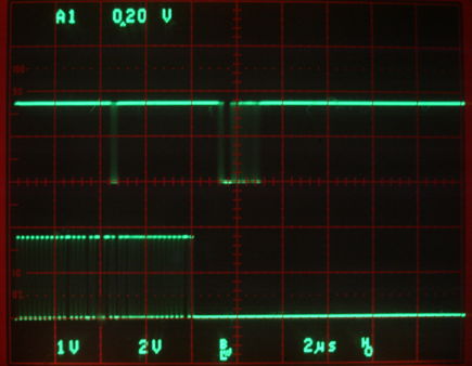
In the figure above, we see the Y1/Y2 signal is by default HI (1). The message incoming notification takes place roughly half-way through the transmitter radio-frequency burst, following eleven start synch bits, a start bit, and eight data bits received. The notification is a serial transmission of the value 0xA, followed by all ones. When the message has been decoded, we have a message data notification, which begins with the value 0xC, followed by the eight-bit channel number, sixteen bits of data, and an eight-bit timestamp. Clock messages are transmitted in a similar way, starting with value 0xB, eight zeros for the clock channel number, the top sixteen bits of the timestamp, and then the A3027 firmware version number.
In order to guarantee that all clock messages stored by the A3027 are transmitted in the notification data stream, all message notifications and incoming notifications are suppressed for 30 μs before each clock message. The clock messages are saved every 7.8 ms, so we miss 0.3% of data messages in this way.
The Message Notifications are designed for use with the Animal Location Tracker (A3032A). The X1 output is set by a LWDAQ command. To set X1 to HI, or 3.3 V, transmit 0x0104. To clear X1 to LO, or 0.0 V, transmit 0x0004. The X2 output is Immediate Sample Transmission, as in Firmware V5.
Firmware V10: Adds support for set numbers. All SCTs belong to a transmitter set between 0 and 13. By default, Firmware V10 responds only to channels 1-14. It is possible to write to a four-bit register on the A3027 to change the set number it records from, although access to this register is not provided by the latest Receiver Instrument or Neurorecorder Tools. Firmware V10 provides a four-bit register space sixteen registers long. The first register, address zero, controls X1. To set or clear X1 we transmit LWDAQ device command 0x0104 and 0x0004 to the A3027 device. To assign the value S to the Set Select Register, we write to the second register, address one, with 0x1s04, s is the hexadecimal representation of S. The remaining fourteen registers are available for future use. If we write value 0xF (decimal 15) to the Set Select Register, the A3027 will accept messages from all sets. If two transmitters have the same channel number, but different set numbers, their signals will be combined into the same channel. For example, channel 17 and channel 1 will be combined into channel 1. The X2 output is Immediate Sample Transmission, as in Firmware V5.
Firmware V11: Supports channel numbers 1-254 as described here. By default, however, FV11 responds only to channels 1-14. Identical to firmware V10 except for two changes. The set number is always stored in the top four bits of the channel number. When all sets are being recorded, duplicate messages are not elimiated. If eight antennas receive the same message, eight copies will be stored. The Receiver Instrument ipurges duplicates as soon as it receives them, but they must still be downloaded. Immediate sample transmission as for FV = 5.
Firmware V12: Supports channel numbers 1-254 as described here. By default, however, FV12 responds only to channels 1-14. Duplicate reduction replaces duplicate elimination. We remove >99% of duplicates. The remaining duplicates are eliminated by the Receiver Instrument. The X2 output is Immediate Sample Transmission, as in Firmware V5.
If your Octal Data Receiver (A3027) is equipped with Firmware V12, you will be able to record from all channel numbers 1-254, but only after the Receiver Instrument or Neurorecorder Tool has configured the A3027 to accept all channel numbers. Modern Receiver Instrument and Neurorecorder Tools automatically configure your A3027 to record from all channel numbers 1-254. But if you press the reset button on the front of an A3027 with firmware V12, the firmare will go back to detecting only channel numbers 1-14. This behavior leads to confusion in several situations. If you connect power to your A3027 with FV12, connect an antenna and turn on a transmitter with channel number 1-14, an activity light will illuminate on the front panel. But if you turn on a transmitter with channel number 17-254, no light will turn on, even if the second transmitter is running. Now you use the Receiver Instrument to download data from the first transmitter, and suddenly you see two lights. The A3027 is receiving from both transmitters. Later, you stop downloading. You come back the next day. You turn on both transmitters and both activity lights illuminate. You press the reset button on the A3027, or you unplug and plug in power, and one of the two lights goes off. Or you can imagine having ten transmitters all with channel numbers greater than 14, and you sometimes see activity, sometimes you do not, depending upon whether the A3027 has been reset by the Receiver Instrument or Neurorecorder Tool.
Firmware V13: As V12, but default configuration is to detect all channel numbers, rather than only 1-14. We also correct an error in implementation of antenna activity lights. The X1 output is user logic output as in FV6. The X2 output is Immediate Sample Transmission, as in FV5. The Y1 and Y2 outputs are both dedicated to message notification for location trackers.
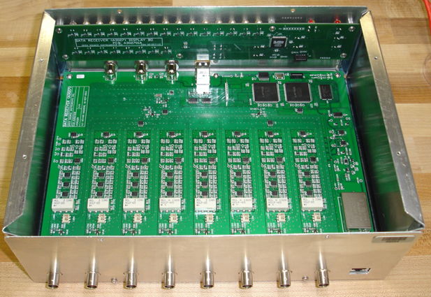
[28-FEB-17] There are three programmable logic chips in the A3027 enclosure. The Message Router chip controls how transmitter messages are stored in memory and uploaded to the LWDAQ Driver. In firmware version xx, the Message Router logic is defined in source file P302701Axx.abl. We program the chip itself with compiled file P302701Axx.jed. The second logic chip is the Message Decoder, which controls how incoming bit sequences are received. The Message Decoder is defined by P302702Axx.abl and programmed by P302702Axx.jed. The third logic chip is the Display Controller, which we define with P302703Axx.abl and program with P302703Axx.jed. The Message Router and Message Decoder are both on the main circuit board inside the A3027 enclosure, and we program them with one operation. The Display Controller chip is on the circuit board behind the display lights, and we program it with its own operation. Most likely, you will not have to upgrade your display board firmware, so the only operation you need to perform to update your A3027 firmware is to re-program the Message Router and Message Decoder on the main circuit board.
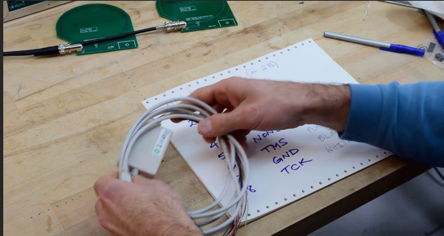
The A3027 logic chips are manufactured by Lattice Semiconductor. To re-program them, you need the programming cable and software. The cable is described on-line here. The programming cable is available from DigiKey and RadioSpares. The Windows version of the programming software you can download here. There is a Linux version also, but we do not maintain a copy of the Linux version ourselves. There is no MacOS version. The programming cable comes with many wires and a single-row eight-way socket adaptor that you use to connect the wires called VCC, TDO, TDI, TMS, GND, and TCK to the circuit you want to re-program. The following movie shows you how to attach the wires to the adaptor.
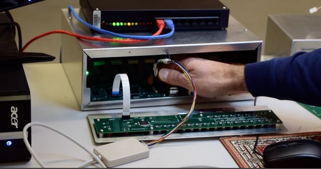
In the programming software, select Help and search for "USB Driver". Follow instructions to install USB port drivers. If the program tells you the drivers are already installed, re-install them. Plug the programming cable into your computer when the installer asks you to do so. Install all versions of the USB driver. Restart the programming software. You are now ready to reprogram the logic chips. In the following movie, we reprogram the two logic chips on the main circuit board.
The software procedure is slightly different for the newer version of the programming software. We demonstrate the newer procedure in the video below.
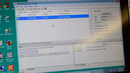
If the software scans the A3027 firmware correctly, but fails to program the firmware afterwards, go into the programmer software settings and adjust the programmer configuration by clicking "continue download on error". We have had to make this adjustment on some virtual Windows machines. The programming will now proceed, but you will get a warning at the end. In our experience, the firmware will be loaded correctly into the A3027 despite the warnings.
The programming software takes JEDEC files as input. The following table provides links to the JEDEC files you need for various firmware versions. In order to show when you have to reprogram the Display Controller, we provide the earliest version of Display Controller firmware that is compatible with each overall firmware version number. Firmware versions 4-12, for example, all use the Display Controller firmware of Firmware Version 4. So if your existing firmeware version is 4 and you are upgrading to 12, you don't need to re-program the Display Controller on the display board.
| Version | Message Router |
Message Detector |
Display Controller |
|---|---|---|---|
| 4 | P302701A04.jed | P302702A04.jed | P302703A04.jed |
| 5 | P302701A05.jed | P302702A05.jed | P302703A05.jed |
| 6 | P302701A06.jed | P302702A06.jed | P302703A06.jed |
| 7 | P302701A07.jed | P302702A07.jed | P302703A07.jed |
| 8 | P302701A08.jed | P302702A08.jed | P302703A08.jed |
| 9 | P302701A09.jed | P302702A09.jed | P302703A09.jed |
| 10 | P302701A10.jed | P302702A10.jed | P302703A10.jed |
| 11 | P302701A11.jed | P302702A11.jed | P302703A11.jed |
| 12 | P302701A12.jed | P302702A12.jed | P302703A12.jed |
| 13 | P302701A13.jed | P302702A13.jed | P302703A13.jed |
Determine the firmware version of your A3027 by looking at the Receiver Instrument panel, where there is a firmware version display box. The firmware version will be displayed with 30 added to it, so 42 is firmware version 12.
Once you have downloaded the JEDEC files you need, scan the programming connector on the A3027 with the programming cable using the Scan button in the programming software. A new window will open and you will see two logic chips listed in the programming cable window. By clicking on the file entry box next to each logic chip, you can associate each chip with a JEDEC file. The first chip listed is the Message Router, which takes the 01Axx.jed files and the second is the Message Decoder, which takes the 02Axx.jed files. Press Go and the programming begins. When it is done, unplug the cable and test the A3027. You can reprogram the firmware as often as you like.
[28-JUN-25] There are a total of thirty indicator lamps on the front panel of the Octal Data Receiver (A3027). Fifteen of them along the top are Channel Activity lamps. These are numberd 1-15. Those numbered 1-14 are white. The 15th is blue. These lamps turn on when samples are received on certain telemetry channels. Any of the channel numbers 1-254 can be used for telemetry, excepting those channel numbers that are exactly divisible by 16. If we turn on a transmitter, one of the activity lights will turn on. Given a transmit channel number, we determine which activity light will turn on by dividing the channel number by sixteen and taking the remainder. The remainder gives us the activity lamp number that will illuminate. So channels 1, 17, 33, and 49 all cause activity lamp number one to turn on. Channels 14 and 94 both cause lamp number fourteen to turn on. Lamp number 15 is for channel numbers with remainder 15. This lamp is blue, because all these channel numbers are reserved for metadata transmission. Metadate transmission are used by Implantable Stimulator-Transponders (ISTs) for acknowledgements and reporting.
If you find that your channel and antenna activity lamps are behaving erratically, check the firmware version of your A3027. For example, if the activity lamps for some of your transmitters turn on, and then after you press the reset button on the A3027, they turn off, or they turn off after you unplug and plug in the network cable at the back of the A3027. Or perhaps you notice that, as soon as you contact the A3027 with the Receiver Instrument or Neurorecorder Tool, some of the activity lights turn on. You will see the firmware version reported in both the Receiver Instrument and the Neuroplayer Tool. If your A3027 has Firmware V12, lamps will illuminate for channels greater than fifteen only after you configure the A3027 using the Receiver Instrument or Neurorecorder Tool. After you press the A3027's reset button, Firmare V12 will stop recording channel numbers greater than fifteen, so lamps corresponding to these channels will extinguish.
The A3027 channel activity lamps shine with a brightness proportional to the number of samples being received on corresponding channels per second. The brightest they will get is when we are receiving roughlky 2048 SPS. If two transmitters with 512 SPS are sharing the same channel activity lamp, we will be able to tell when we turn one of them on and off because the lamp will get brighter and dimmer.
There are eight Antenna Activity lamps, one for each of the eight antenna inputs on the A3027. These shine in proportion to the number of samples being received by each of the eight inputs. They show us which antennas are receiving telemetry signals. The remaining indicator light are for power, reset, activity, and empty data buffer. Press the HIDE button and all lamps except HIDE and the power lamps will turn off. Turning off the lamps reduces disturbance to the animals at night.
[27-JUN-25] For design files and development logbook, see the A3027 design and development page at D3027.