| Description |
| Applications |
| Assembly Language |
| Status Flags |
| Instruction Set |
| Assembler |
| Set-Up |
| Current Consumption |
| Speed |
| Design |
[12-JUN-26] The OSR8 is an open-source, reconfigurable eight-bit processor described in VHDL (Virtual Hardware Description Language). You will find the source code in the OSR8 Git repository here. The OSR8 is designed for use in miniature, micropower devices. When deployed in the LCMXO2-1200ZE, the OSR8V4 occupies 800 of the device's 1280 available four-bit look-up tables (LUTs). It will runs at a clock speed of up to 8 MHz in these chips. The OSR8 consumes roughly 1.1 mA from a 1.2-V power supply running at 5 MHz and performing one hundred and fifty thousand eight-bit multiplications per second. The OSR8 is designed to work with a a 5-MHz ring oscillator, a micropower 32.768 kHz oscillator, and a clock selector. The ring oscillator turns on and off instantly. The clock selector allows us to move the OSR8 from the slow to the fast clock within a few hundred nanoseconds and back again in a few microseconds. By operating in bursts, the OSR8 minimizes its average current consumption.
The OSR8 provides seven eight-bit registers, A, B, C, D, E, H, and L, and a flags register, F. The flags are zero (Z), sign (S), carry (C), and interrupt (I). It provides two index registers, IX and IY, that hold process memory pointers for moving bytes between process memory and the registers. It provides a stack pointer, SP, and push and pop operations for all seven registers. A program counter, PC, steps through instructions in program memory and jumps to subroutines and interrupts. There are separate increment and decrement functions for registers A, B, C, and D, as well as IX and IY. The H and L registers together make a sixteen-bit register HL. We can load SP or PC with HL, and we load HL with SP, PC, or a constant. The arithmetic logic unit (ALU) provides eight-bit addition and subtraction of registers A and B, and of A and a constant, with and without carry in. The ALU also provides a variety of shift and rotate operations that facilitate multiplication and long addition, as well as logical AND, OR, and XOR between A and B, or between A and a constant. The OSR8 assembly language is similar to that of the Z80 in the way the instructions are written out. Unlike the Z80, however, the OSR8 uses big-endian byte ordering and its stack extends upwards rather than downwards. When we push a byte onto the OSR8 stack, we increment the stack pointer and write the byte tolocation pointed to by the incremented stack pointer. When we push a two-byte index register, we push the most significant byte first, so that it is at the lower address.
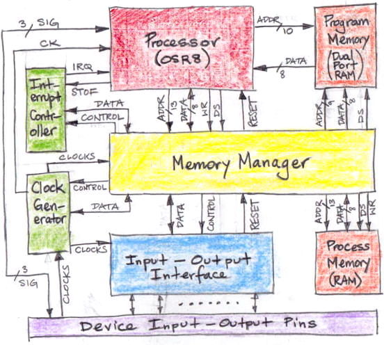
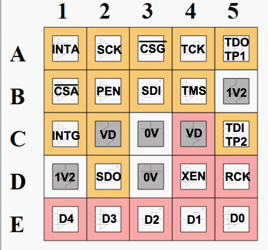
The processor is a single VHDL entity implemented entirely with look-up tables and registers. It communicates with the outside world through the signals shown in the diagram above. All other components of the embedded controller are provided by entities peripheral to the OSR8, but residing within the firmware of the logic chip, or by components external to the logic chip. In the A3041A, for example, the program memory, process memory, interrupt timers, and sensor interfaces are all peripheral to the OSR8, because they are implemented by logic within the same LCMXO2-1200ZE logic chip, while the sensors themselves are external, because they are provided by components outside the logic chip. The program memory contains the instructions that will be executed by the processor. The processor reads from the program memory with its program counter. The processor accesses all other peripherals through an external memory management unit (MMU) by means of the processor address and data buses. The processor implements a bi-directional eight-bit data bus with eight outgoing data bits and eight incoming data bits. The processor uses the rising edge of its clock to set up its program counter, processor address, outgoing processor data, and all control signals. It uses the rising edge to store incoming processor data. In all existing OSR8 applications, we read the program memory on the falling edge of CK. The memory manager should act on the falling edge of CK for read cycles, and can use the falling edge or rising edge of CK for write cycles. By using both edges of CK, the processor is able to perform register-only instructions in one clock cycle. When the MMU implements a program memory that the process can write to, the processor read cycles must take place on the opposite edge from the write cycles. We read instruction bytes from propram memory on the falling edge of CK and write instructions into the user program memory on the rising edge.
Some OSR8 applications, such as the A3035, provide no connection between the memory manager and the program memory. The processor runs only programs that were written to its non-volatile configuration memory at the time the device was programmed. The device may not be reprogrammed once it is encapsulated. Others, such as A3041 A3054 provide write-only access to an upper portion of the program memory through the memory manager. These devices can receive programs through their crystal radios and write them to the program memory for execution. In the case of the A3054, these programs can be stored in the device's separate non-volatile memory and transferred into program memory on power-up, so that the device does not forget the programs we upload to it.
The Interrupt Request (IRQ) input interrupts the processor, provided the processor's interrupt flag (I) is not set. The interrupt controller provides interrupt bits for various interrupt sources, mask bits to enable or disable assertion of IRQ by these individual interrupt bits, as well as set and reset bits that the processor can use to clear and assert interrupts. The A3041 application provides two sixteen-bit delay timer interrupts and two eight-bit periodic interrupt clocks. The OSR8 provides an Interrupt Service (ISRV) output that indicates the CPU is servicing an interrupt.
The RESET input to the processor will reset its stack pointer and program counter and re-start program execution from the starting address. In the A3035A, the start address is 0x0000, and the interrupt address, to which the processor jumps upon servicing an interrupt, is 0x0003. Both locations should be occupied by an unconditional jump instruction that takes the processor to the correct program. The OSR8 "jp nn" instruction occupies three bytes. The OSR8 has no reset instruction. The A3035A application provides a software reset bit the processor can set to cause RESET to be asserted for one CK period. Additional internal controller functions may be added and made available to the OSR8 through the Memory Manager. The A3037B provides an eight-bit multiplier to accelerate EEG signal analysis. The processor writes two bytes to two locations, and reads our the product from to additional locations.
The input-output pins are the signals present on the device pins. These pins constitute the input-output interface. They provide access to external circuit components. In the A3035A application, the interface provides logic to read and write from an accelerometer and a gyroscope, and to transmit sixteen-bit samples through the radio-frequency antenna. These functions are made available to the processor by the memory manager in the form of eight-bit memory locations. To write a sixteen-bit word to the accelerometer, for example, the processor writes the high and low bytes to two separate locations, the accelerometer register address to a third location, and a code number to a control register to initiate the write cycle. In the A3037B, the processor turns on the implantable lamp attached to the A3037B's stimulus leads by writing to a register, and turns off the lamp by writing to the same register. The processor provides three re-configurable signals SIG0..SIG2 that may be connected directly to the device pins. In the A3035A, these three signals are outputs that encode the state of the processor, and so may be used for debugging program execution. But the SIG signals could be re-configured to act as copies of internal CPU signals, or as inputs to the CPU for new instructions added to the OSR8 for new applications.
One of our chief concerns with the OSR8 is its size: we want it to occupy as little logic as possible while maintaining an instruction set that allows all compute functions to be executed, even if they must be executed with a large number of instructions. We might wonder what is the use of keeping the E register, when it has no special function, and no increment or decrement. The reason we keep it is because the size of the OSR8 when compiled by Synplify Pro is 20 LUTs smaller with register E included than with it excluded. Why this should be, we have not yet determined, but it is a fact, so we keep E, and we sometimes use it for short-term storage of values.
[12-JUN-26] The processor is defined in a single VHDL file OSR8Vn.vhd, where n is version number. We configure the OSR8 with generic constants when we instantiate the CPU in our firmware architecture. The table below lists some applications of the OSR8. Click on the OSR8 link to go to the device's firmware repository.
| Version | Platform | Size (LUTs) |
Features | Application with Clock Frequency |
|---|---|---|---|---|
| OSR8 | Any | 800 | User-Configurable | All active versions of the OSR8 |
| OSR8V3 | LCMXO2-1200ZE WLCSP-25 | 800 | 1 KB RAM, 4 KB ROM, 5.0 MHz. | Implantable Inertial Sensor (A3035) |
| OSR8V3 | LCMXO2-7000HC TQFP-144 | 950 | 6 KB RAM, 8 KB ROM, 20 MHz. | Animal Location Tracker Base Board (A3038) |
| OSR8V4 | LCMXO2-1200ZE WLCSP-25 | 850 | 1 KB RAM, 4 KB ROM, 5.0 MHz with user program memory |
Implantable Stimulator-Transponder (A3041) |
| OSR8V3 | LCMXO2-7000HC TQFP-144 | 850 | 2 KB RAM, 4 KB ROM, 20 MHz | Telemetry Control Box Base Board (A3042BB) |
| OSR8V3 | LCMXO2-1200ZE WLCSP-25 | 800 | 1 KB RAM, 4 KB ROM, 5 MHz. | Fiber Controller (A3045) |
| OSR8V3 | LCMXO2-1200ZE QFN-32 | 800 | 1 KB RAM, 4 KB ROM, 5 MHz. | Blood Pressure Monitor (A3051) |
| OSR8V4 | LCMXO2-1200ZE QFN-32 | 800 | 1 KB RAM, 4 KB ROM, 5 MHz. | Intraperitoneal Transmitter (A3054) |
The peripheral functions of each application are defined in separate files specific to the application. The links in the application column of the table above lead to circuit manuals.
Here is an example OSR8 program written in the OSR8 Assembly Language. When this program runs in the A3035A application, it generates a square wave on pin P1-1 of the programming extension.
const mmu_tpr  0x1E38 ; Test Point Register
main:
ld A,0x01        ; 2 Load A with bit zero set to one.
ld (mmu_tpr),A   ; 3 Set the test point one bit.
ld A,0x00        ; 2 Load A with all bits zero.
ld (mmu_tpr),A   ; 3 Clear the test point one bit.
jp main          ; 3
The program begins with the declaration of a sixteen-bit constant giving the address in process memory of the test point register, which the OSR8 can use to set the logic level on TP1 in the A3035A. The main loop sets bit zero of the test point register to HI and then LO before jumping back to start over. We show the number of clock cycles used by each instruction in the loop. The entire loop takes 13 clock cycles, and the clock is 32.768 kHz so the square wave will run at 2.52 kHz and its HI pulse will be 152 μs.
In OSR8 assembly, each instruction is presented on a single line of assembly code. The first word in an instruction line is the operation code, or opcode. After that there may be two operands separated by commas. We use parenthesis to show that an operand should be used as an address to access a byte in process memory. When we load a register with the operand itself, we refer to the operation as a direct load. When we use the operand as an address to look up a value to load into a register, we refer to the operation as an indirect load. Thus "ld A,4" is a direct load of register "A" with the constant "4", while "ld A,(0x0123)" is an indirect load of register "A" with the contents of memory address "0x0123". On any line, every character after a semicolon is a comment and will be ignored by the assembler. The language is insensitive to case, so you may use lower-case or upper-case letters as you like. The following line specifies the eight-bit indirect load of the accumulator from address 0x1702.
ld A,(0x1702) ; Load A with HI sensor byte.
We specify a location in program memory to which we can jump to, we use any any string containing letter and underscores followed immediately by a colon, and place this label just before the location we wish to label. The label must be alone on its declaration line. When we later mention the label, we do not include the colon, so as to distinguish between the definition of the label and the use of the label.
loop:        ; We can put a comment here too
dec A        ; Decrement the accumulator
jp nz,loop   ; Jump to loop if accumulator is not zero
Jump points are global constants that can be declared anywhere and referred top anywhere. So we can refer to a jump point in an instruction before we declare it.
dec l       ; Decrement register L
jp nz,notz  ; If L is not zero, jump over the decrement of H
dec h       ; Decrement register H
notz:       ; This is where we declare the label "notz"
adc A,56    ; Add 56 decimal to the accumulator, with carry.
Empty lines, or lines with only comments, are ignored by the assembler, although they are counted, so that warning and error messages will be able to refer to the correct line number. To declare a constant use the following notation.
const sensor_hi 0x1702 ; Define sensor_hi to be value 1702 hexadecimal.
const step_size 34     ; Replace "step_size" with 34 decimal.
ld A,step_size         ; Load step-size constant into the accumulator
ld (sensor_hi),A       ; Load byte location sensor_hi with accumulator.
All constants in OSR8 assembly are global constants and must be declared before they are used. All labels are global labels, but they may be declared after they are used. In the following program, we see the labels "main" and "interrupt" are used before they are defined.
start:
jp main
jp interrupt
interrupt:
rti
main:
jp main
The "start" label marks the address at which program execution will begin. In the A3035A application, this address is 0x0000. When the OSR8 is interrupted by IRQ or an "int" instruction, it jumps to a pre-defined interrupt address in program memory. In the A3035A application, this interrupt address is 0x0003. The value 0x0003 is convenient because the "jp main" instruction occupies three bytes, so the "jp interrupt" we can put immediately after "jp main" and the two instructions will be correctly located in program memory for start-up and interrupts. We see that the "main" and "interrupt" labels are referenced before they are defined.
[01-JUL-22] The OSR8 status flags are zero (Z), sign (S), carry (C), and interrupt (I). Mathematical and logical operations set the flags. Load, push, and pop operations do not. In our description of each instruction, we state which flags the instruction sets. We present the flags in detail here. The Z, S, and C flags are set by the action of the OSR8's arithmetic logic unit (ALU). The ALU is an eight-bit adder, subtractor, and logical operator. The Z flag is set when the eight-bit result of an operation is all zeros. Here are some examples.
and A,0xFF ; When A=0, Z will be set.
add A,0 ; When A=0, Z will be set.
sub A,7 ; When A=7, Z will be set.
xor A,0xFF ; when A=0.FF, Z will be set.
add A,0 ; When A=1, Z will not be set.
add A,1 ; When A=0xFF will be set.
When the result of an addition overflows the eight-bit output of the ALU, a ninth bit, called the carry bit is set, as if the output of the ALU were a nine-bit number. When the result of subtraction underflows zero, the carry bit is once again set, to represent a borrow bit. The C flag is set whenever this carry or borrow bit is set. When we add one to 0xFF we get 0x00 with the carry bit set. So we have the Z flag set, and we also have the C flag set.
and A,0xFF ; C will never be set.
add A,0 ; C will never be set.
sub A,7 ; When A<7, C will be set.
add A,23 ; When A>=233, C will be set.
The S flag is for two's-compliment arithmetic, where we represent negative integers by taking the positive integer, negating its bits and adding one. We would negate an integer like this:
xor A,0xFF ; Negate all bits
add A,1 ; and add one.
In the above example, +1 becomes 0xFF, which is the two's compliment representation of −1. When we add +1 and −1 together we get zero with a carry. The eight-bit ALU inputs and outputs, when used for signed integert arithmetic, represent values −128 to +127. The negative values are those with the top bit set. The S flag is set equal to the top bit of the ALU result after a mathematical or logical operation. We intend the N flag to mean, "The result of the most recent two's compliment addition or subtraction is less than zero".
The OSR8 provide conditional jump commands controlled by the Z, S, and C flags. The "S" flag we refer to in these commands with "p" for "positive" and "np" for "not positive". By "positive" we mean "zero or greater", which is "0..127". By "not positive" we mean "less than zero".
ld A,65 ; Load 0x41 into A.
add A,76 ; Add 0x4C to A. Sum is 141, 0x8D, or -115.
jp np,later ; We will jump.
The I flag is the "CPU running in interrupt mode" flag. The I flag is set automatically by the execution of an interrupt, but we can also set it with the seti instruction, and clear it with clri. When the CPU sets I, we think of it as saying that it is already handling an interrupt, so no other interrupt should do any further interrupting. When we clear the I flag, we are saying that interrupt handling is over, and a new interrupt can commence.
[17-FEB-26] The OSR8 is a Reduced Instruction Set Computer (RISC). Many instructions execute in one clock cycle, and none take more than four clock cycles. The instruction set is, we believe, sufficient to perform any arithmetic or multi-tasking function. There are seven working registers A, B, C, D, E, H, and L. There is also a flags register, F, that contains the zero, sign, carry, and interrupt flags. All of these can be pushed onto the stack or popped off the stack. Registers A, B, C, and D can be incremented or decremented. There are two index registers, IX and IY, which can be incremented or decremented. The stack pointer, SP, and program counter, PC, can by copied to and from the combined registers HL. We can load a two-byte value into HL as well. Register A can be loaded with a byte value, a byte from a sixteen-bit memory location, or from a memory location pointed to by IX or IY. We can write A to a memory location or to the locations pointed to by IX and IY. We can and, or, xor, add, or subtract A with a value or with the contents of register B. We can perform a variety of different shifts and rotations on A as well. There are no instructions to move the contents of one register to another: we use the stack to perform such moves, by pushing one register onto the stack, and popping the other. The "call" instruction jumps to a subroutine and a "ret" instruction returns from the subroutine to the instruction after the call. The OSR8 supports a single interrupt routine location, which the processor will jump to when it sees its interrupt request line asserted. We use the "rti" instruction to return from an interrupt to continue execution where we left off. When the interrupt flag is set, interrupts are disabled.
| Syntax | Opcode | Cycles | Syntax | Opcode | Cycles | Syntax | Opcode | Cycles | Syntax | Opcode | Cycles |
|---|---|---|---|---|---|---|---|---|---|---|---|
| nop | 0x00 | 1 | jp nn | 0x01 | 3 | jp nz,nn | 0x02 | 3 | jp z,nn | 0x03 | 3 |
| jp nc,nn | 0x04 | 3 | jp c,nn | 0x05 | 3 | jp np,nn | 0x06 | 3 | jp p,nn | 0x07 | 3 |
| call nn | 0x08 | 3 | ret | 0x0A | 4 | rti | 0x0B | 3 | wait | 0x0C | 1 |
| clri | 0x0D | 1 | seti | 0x0E | 1 | ld A,n | 0x10 | 2 | ld IX,nn | 0x11 | 3 |
| ld IY,nn | 0x12 | 3 | ld HL,nn | 0x13 | 3 | ld A,(nn) | 0x14 | 4 | ld (nn),A | 0x15 | 3 |
| ld A,(IX) | 0x16 | 2 | ld A,(IY) | 0x17 | 2 | ld (IX),A | 0x18 | 1 | ld (IY),A | 0x19 | 1 |
| ld HL,SP | 0x1A | 1 | ld SP,HL | 0x1B | 1 | ld HL,PC | 0x1C | 1 | ld PC,HL | 0x1D | 1 |
| push A | 0x20 | 1 | push B | 0x21 | 1 | push C | 0x22 | 1 | push D | 0x23 | 1 |
| push E | 0x24 | 1 | push H | 0x25 | 1 | push L | 0x26 | 1 | push F | 0x27 | 1 |
| push IX | 0x28 | 2 | push IY | 0x29 | 2 | pop A | 0x30 | 2 | pop B | 0x31 | 2 |
| pop C | 0x32 | 2 | pop D | 0x33 | 2 | pop E | 0x34 | 2 | pop H | 0x35 | 2 |
| pop L | 0x36 | 2 | pop F | 0x37 | 2 | pop IX | 0x38 | 3 | pop IY | 0x39 | 3 |
| add A,B | 0x40 | 1 | add A,n | 0x41 | 2 | adc A,B | 0x42 | 1 | adc A,n | 0x43 | 2 |
| sub A,B | 0x44 | 1 | sub A,n | 0x45 | 2 | sbc A,B | 0x46 | 1 | sbc A,n | 0x47 | 2 |
| clrf | 0x4F | 1 | inc A | 0x50 | 1 | inc B | 0x51 | 1 | inc C | 0x52 | 1 |
| inc D | 0x53 | 1 | inc IX | 0x59 | 1 | inc IY | 0x5A | 1 | dec A | 0x60 | 1 |
| dec B | 0x61 | 1 | dec C | 0x62 | 1 | dec D | 0x63 | 1 | dly A | 0x67 | A |
| dec IX | 0x69 | 1 | dec IY | 0x6A | 1 | and A,B | 0x70 | 1 | and A,n | 0x71 | 2 |
| or A,B | 0x72 | 1 | or A,n | 0x73 | 2 | xor A,B | 0x74 | 1 | xor A,n | 0x75 | 2 |
| rl A | 0x78 | 1 | rlc A | 0x79 | 1 | rr A | 0x7A | 1 | rrc A | 0x7B | 1 |
| sla A | 0x7C | 1 | sra A | 0x7D | 1 | srl A | 0x7E | 1 |
The assembler lists all instructions defined by all versions of the OSR8. Before we attempt to include instructions in our assembly code for a particular OSR8 application, we must make sure that the application's OSR8 version provides the instruction. We define the complete set of instructions below. For each instruction, we state what flags are affected by the instruction, and how they are affected. If we do not mention a flag in the description of an instruction, it is unaffected. We also give the number of clock cycles required to execute the instruction.
nop: No operation. Increment the program counter and read the next operation code. Clock cycles: 1.
jp nn: Unconditional jump to location nn in program memory, where nn is a two-byte address. Clock cycles: 3.
jp nz,nn: If the zero flag (Z) is not set, jump to location nn, otherwise proceed to the next instruction. Clock cycles: 3.
jp z,nn: If the zero flag (Z) is set, jump to location nn, otherwise proceed to the next instruction. Clock cycles: 3.
jp nc,nn: If the carry flag (C) is not set, jump to location nn, otherwise proceed to the next instruction. Clock cycles: 3.
jp c,nn: If the carry flag (C) is set, jump to location nn, otherwise proceed to the next instruction. Clock cycles: 3.
jp np,nn: If the sign flag (S) is set, jump to location nn, otherwise proceed to the next instruction. The sign flag is set when the result of an addition, subtraction, or decrement is negative in two's compliment arithmetic, which is true if and only if the top bit of the eight-bit result was set. The pneumonic "np" means "not positive". We cannot use "n" for "negative condition" and "nn" for "not negative", because we have already reserved these letters in our pneumonic definitions. So we use "p" for positive and "np" for not positive. Clock cycles: 3.
jp p,nn: If the sign flag (S) is not set, jump to location nn, otherwise proceed to the next instruction. See above for why we use "p" for "not negative". Clock cycles: 3.
call nn: Call the subroutine that begins at program location nn. The OSR8 will push the program counter onto the stack, HI byte first, LO byte second, then jump to the specified location. Clock cycles: 3.
ret: Return from subroutine. Pop the program counter off the stack, LO byte first, HI byte second, increment the program counter, and so execute the next intruction after the "call" instruction we assume was used to execute the subroutine from which we are returning with "ret". Clock cycles: 4.
rti: Return from interrupt. Pop the program counter off the stack, LO byte first, HI byte second. We are returning from executing the interrupt routine. We jump to the interrupt routine in response to IRQ being asserted. The OSR8 performs the jump in place of the next opcode it loads. It does not execute the loaded opcode. Instead, it sets the interrupt flag, I, and pushes the program counter onto the stack. Upon encountering rti in the interrupt routin, the OSR8 pops the program counter off the stack, does not increment the program counter, clears I, and continues execution of the interrupted process with the instruction it was about to execute when it jumped to the interrupt. If we want to execute an interrupt routine from software, without IRQ being asserted, we can do so in the following way. We create a label in our assembly code pointint to the location at which we want execution to continue after we return from the interrupt routine. Call it "loc". Now we do "ld HL,loc; push L; push H; seti; jp interrupt". Here "interrupt" is the location of the interrupt routine, and we using semicolons to separate the instructions, even though we need newlines in the OSR8 assembly language. Now the rti at the end of the interrupt will pop the "loc" off the stack and load it into the program counter. It will clear I, and continue exacution at "loc". Clock cycles: 3.
wait: Clear the I flag so as to enable interrupts, but otherwise do nothing. Do not increment the program counter, but keep executing this instruction until IRQ or RESET is asserted. When IRQ is asserted, execute the interrupt routine, then return to the wait instruction. Clock cycles: 1.
clri: Clear the I flag to zero, thus enabling interrupts. Clock cycles: 1.
seti: Set the I flag to one, thus disabling interrupts. Clock cycles: 1.
ld A,n: Direct load of A. Load register A with the single-byte value n. Clock cycles: 2.
ld IX,nn: Direct load of IX. Load index register IX with two-byte process address value nn. Clock cycles: 3.
ld IY,nn: Direct load of IY. Load index register IY with two-byte process address value nn. Clock cycles: 3.
ld HL,nn: Direct load of HL. Load register pair HL with two-byte constant nn, where the HI byte of the constant is loaded into H and the LO byte is loaded into L. Clock cycles: 3.
ld A,(nn): Indirect load of A. Read the byte at process memory location nn and load it into register A. Clock cycles: 4.
ld (nn),A: Indirect load from A. Write the byte in register A to location nn in process memory. Clock cycles: 3.
ld A,(IX): Indexed load of A using IX. Read the byte at location IX in process memory and load it into A. Clock cycles: 2.
ld A,(IY): Indexed load of A using IY. Read the byte at location IY in process memory and load it into A. Clock cycles: 2.
ld (IX),A: Indexed load from A using IX. Write the byte in register A to location IX in process memory. Clock cycles: 1.
ld (IY),A: Indexed load from A using IY. Write the byte in register A to location IY in process memory. Clock cycles: 1.
ld HL,SP: Direct load of register pair HL with stack pointer SP. The HI byte of the stack pointer, SP, is loaded into H and the LO byte is loaded into L. Clock cycles: 1.
ld SP,HL: Direct load of SP with HL. The HI byte of the stack pointer, SP, is loaded with H, and the LO byte of SP is loaded with L. Clock cycles: 1.
ld HL,PC: Direct load of HL with PC. The HI byte of the program counter, PC, is loaded into H, and the LO byte of PC is loaded into L. Clock cycles: 1.
ld PC,HL: Direct load of PC with HL. The HI byte of the program counter, PC, is loaded with H, and the LO byte of PC is loaded with L. Clock cycles: 1.
push A: Push A onto the stack. Increment the stack pointer, SP, by one and write A to the process memory location given by the incremented value of SP. Clock cycles: 1.
push B: Push B onto the stack. Increments SP by one. Clock cycles: 1.
push C: Push C onto the stack. Increments SP by one. Clock cycles: 1.
push D: Push D onto the stack. Increments SP by one. Clock cycles: 1.
push E: Push E onto the stack. Increments SP by one. Clock cycles: 1.
push H: Push H onto the stack. Increments SP by one. Clock cycles: 1.
push L: Push L onto the stack. Increments SP by one. Clock cycles: 1.
push F: Push the flags register onto the stack. The values of the Z, S, C, and I flags will be copied to the stack. We push the flags onto the stack when we begin an interrupt routine that will change the flags. Increments SP by one. Clock cycles: 1.
push IX: Push IX onto the stack. The HI byte will be pushed first, and the LO byte second. Increments SP by two. Clock cycles: 2.
push IY: Push IY onto the stack. The HI byte will be pushed first, and the LO byte second. Increments SP by two. Clock cycles: 2.
pop A: Pop A off the stack. Read the byte at the process memory location pointed to by the stack pointer and load it into A, then decrement the stack pointer. Decrements SP by one. Clock cycles: 2.
pop B: Pop B off the stack. Decrements SP by one. Clock cycles: 2.
pop C: Pop C off the stack. Decrements SP by one. Clock cycles: 2.
pop D: Pop D off the stack. Decrements SP by one. Clock cycles: 2.
pop E: Pop E off the stack. Decrements SP by one. Clock cycles: 2.
pop H: Pop H off the stack. Decrements SP by one. Clock cycles: 2.
pop L: Pop L off the stack. Decrements SP by one. Clock cycles: 2.
pop F: Pop F off the stack. Pop the flags off the stack. We pop flags off the stack at the end of an interrupt routine that affects the flags. Decrements SP by one. Clock cycles: 2.
pop IX: Pop IX off the stack. The LO byte will be popped first, and the HI byte second. Decrements SP by two. Clock cycles: 3.
pop IY: Pop IY off the stack. The LO byte will be popped first, and the HI byte second. Decrements SP by two. Clock cycles: 3.
add A,B: Add register B to register A, leaving the result in A. If the sum exceeds 0xFF, set the carry flag (C), otherwise clear C. If the sum is zero, set the zero flag (Z), otherwise clear Z. If the sum is negative, set the sign flag (S), otherwise clear S. Clock cycles: 1.
add A,n: Add constant n to register A, leaving the result in A. If the sum exceeds 0xFF, set C, otherwise clear C. If the sum is zero, set Z, otherwise clear Z. If the sum is negative, set S, otherwise clear S. Clock cycles: 2.
adc A,B: Add register B to register A with carry in, leaving the result in A. If C is set, add one to the result. If the sum exceeds 0xFF, set C, otherwise clear C. If the sum is zero, set Z, otherwise clear Z. If the sum is negative, set S, otherwise clear S. Clock cycles: 1.
adc A,n: Add constant n to register A with carry in, leaving the result in A. If C is set, add one to the result. If the sum exceeds 0xFF, set C, otherwise clear C. If the sum is zero, set Z, otherwise clear Z. If the sum is negative, set S, otherwise clear S. Clock cycles: 2.
sub A,B: Subtract register B from register A, leaving the result in A. If the result is less than zero, set C, otherwise clear C. If the result is zero, set Z, otherwise clear Z. If the result is negative, set S, otherwise clear S. Clock cycles: 1.
sub A,n: Subtract constant n from register A, leaving the result in A. If the result is less than zero, set C, otherwise clear C. If the result is zero, set Z, otherwise clear Z. If the result is negative, set S, otherwise clear S. Clock cycles: 2.
sbc A,B: Subtract register B from register A with borrow in, leaving the result in A. If C is set, subtract one from the result. If the result is less than zero, set C, otherwise clear C. If the result is zero, set Z, otherwise clear Z. If the result is negative, set S, otherwise clear S. Clock cycles: 1.
sbc A,n: Subtract constant n from register A with borrow in, leaving the result in A. If C is set, subtract one from the result. If the result is less than zero, set C, otherwise clear C. If the result is zero, set Z, otherwise clear Z. If the result is negative, set S, otherwise clear S. Clock cycles: 2.
clrf: Clear the arithmetic flags Z, S, and C to zero. Clock cycles: 1.
inc A: Increment register A. If the result is zero, set Z, otherwise clear Z. If the result is negative, set S, otherwise clear S. Clock cycles: 1.
inc B: Increment register B. If the result is zero, set Z, otherwise clear Z. If the result is negative, set S, otherwise clear S. Clock cycles: 1.
inc C: Increment register C. If the result is zero, set Z, otherwise clear Z. If the result is negative, set S, otherwise clear S. Clock cycles: 1.
inc D: Increment register D. If the result is zero, set Z, otherwise clear Z. If the result is negative, set S, otherwise clear S. Clock cycles: 1.
inc IX: Increment index register IX. Clock cycles: 1.
inc IY: Increment index register IY. Clock cycles: 1.
dec A: Decrement register A. If the result is zero, set Z, otherwise clear Z. If the result is negative, set S, otherwise clear S. Clock cycles: 1.
dec B: Decrement register B. If the result is zero, set Z, otherwise clear Z. If the result is negative, set S, otherwise clear S. Clock cycles: 1.
dec C: Decrement register C. If the result is zero, set Z, otherwise clear Z. If the result is negative, set S, otherwise clear S. Clock cycles: 1.
dec D: Decrement register D. If the result is zero, set Z, otherwise clear Z. If the result is negative, set S, otherwise clear S. Clock cycles: 1.
dly A: Delay for A clock cycles. Decrement A and execute this instruction again if A is not zero, move on to the next instruction if A is zero. Clock cycles: A.
dec IX: Decrement index register IX. Clock cycles: 1.
dec IY: Decrement index register IY. Clock cycles: 1.
and A,B: Replace A with the logical AND of A and B, where we replace bit b in A with the logical AND of register A bit b and register B bit b for b = 0 to 7. If the result is zero, set Z, otherwise clear Z. Clock cycles: 1.
and A,n: Replace A with the logical AND of A and a constant n. If the result is zero, set Z, otherwise clear Z. Clock cycles: 2.
or A,B: Replace A with the logical OR of A and B. If the result is zero, set Z, otherwise clear Z. Clock cycles: 1.
or A,n: Replace A with the logical OR of A and a constant n. If the result is zero, set Z, otherwise clear Z. Clock cycles: 2.
xor A,B: Replace A with the logical XOR of A and B. If the result is zero, set Z, otherwise clear Z. Clock cycles: 1.
xor A,n: Replace A with the logical XOR of A and a constant n. If the result is zero, set Z, otherwise clear Z. Clock cycles: 2.
rl A: Rotate A left. A(7..1) := A(6..0), A(0) := C (carry bit), C := A(7). Clock cycles: 1.
rlc A: Rotate A left circular. A(7..1) := A(6..0), A(0) := A(7), C := A(7). Clock cycles: 1.
rr A: Rotate A right. A(6..0) := A(7..1), A(7) := C, C := A(0). Clock cycles: 1.
rrc A: Rotate A right circular. A(6..0) := A(7..1), A(7) := A(0), C := A(0). Clock cycles: 1.
sla A: Shift A left arithmetic. A(7..1) := A(6..0), A(0) := 0, C := A(7). Clock cycles: 1.
sra A: Shift A right arithmetic. A(6..0) := A(7..1), A(7) := A(7), C := A(0). Clock cycles: 1.
srl A: Shift A right logical. A(6..0) := A(7..1), A(7) := 0, C := A(0). Clock cycles: 1.
[15-DEC-20] The OSR8 Assembler Tool takes an OSR8 assembly language text file and translates it into a hexadecimal object file that we can use to populate the OSR8's program memory. This translation process we call assembly. The assembler's default output format is a hexadecimal memory file, as defined by Lattice Semiconductor's Lattice Diamond software. The object file consists of a separate hexadecimal byte value on each line, written as two ASCII hexadecimal charcters. The OSR8 Assembler is available in the LWDAQ Tools/More menu. You can download the latest release of LWDAQ here, or get the pre-release version here.
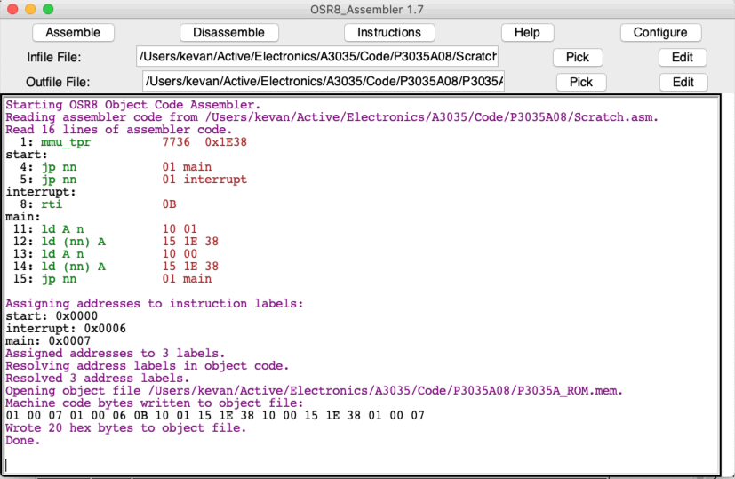
In the above screen shot, we the output of the OSR8 Assembler for our tpreg0_demo.asm demonstration program. The OSR8 Assembler will also perform dis-assembly, where we take the hexadecimal memory file and translate it into OSR8 assembly language. The Pick buttons allow us to select input and output files for the assembler. The Edit buttons opens the corresponding file in a black-and-white editor with copy, paste, save and undo key bindings. Save from the editor and press Assemble to assemble the input file and re-write the output file.
The Instruction button prints out all the instructions known to the assembler. The assembler gets its list of instructions from the OSR8 source file. We cut and paste the instruction definitions directly from the VHDL source code and into the data section of the ORS8 Assembler script. When the assembler starts up, it parses the VHDL definition and creates a list of instruction pneumonics and opcodes. If we modify the OSR8 so as to eliminate instructions or add new ones, we can re-configure our OSR8 assembler easily by over-writing the OSR8_Assembler.tcl data section with the new VHDL instruction definition list.
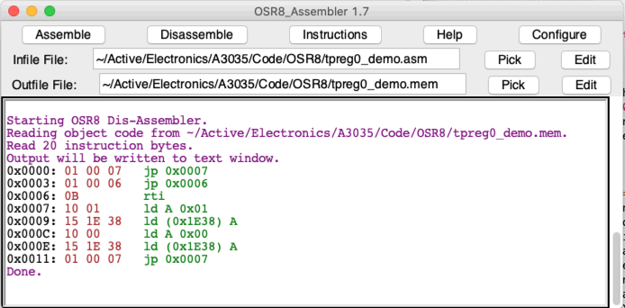
Press the Disassemble button and the tool will read in the output file and generate an assembly-language version of the object code using the instruction pneumonics. There will be no constant definitions: all constants are replaced by their actual hexadecimal values. The disassembler allows us to check that the assembler is working, or that our constant declarations are working.
[19-JAN-21] To illustrate how we can implement the OSR8 processor in a programmable logic chip, we will use the example of the A3035A application. Download OSR Demonstration archive and decompress. You will get a folder P3035 which contains all the files you need to compile the P3035A09 firmware for the A3035A assembly. Install the Lattice Diamond compiler. We built the demonstration on Lattice Diamond version 3.11.3.469. Start Lattice Diamond by double-clicking on the P3035.ldf file.
The P3035 project compiles code for the LCMXO2-1200ZE logic device in a WLCSP25 package. The Main.vhd is the top-level source file. It defines the memory manager, interrupt handler, input-output interface, and clock generator. It uses OSR8V3 to define the processor, and three other automatically-generated files to define the process memory, program memory, and eight-bit multiplier. The program memory is initialized from P3035A_ROM.mem, which you will find in the OSR8_Demo folder. We generate P3035A_ROM.mem with the OSR Assembler tool. Download tpreg0_demo.asm, open the assembler and use it to generate a new copy of P3035A_ROM.mem from tpreg0_demo.asm. In the Lattice Diamond project, double-click on P3035A_ROM.ipx in the File List. A window opens. Press Generate, and the compiler will take the MEM file and use it to construct a new P3035A_ROM.vhd file. You can look at the VHD file and see that it defines the contents of a 1-KByte read-only memory to be implemented in one of the LCMXO2-1200ZE's seven embedded memory blocks. Now synthesize, map, and generate the design. You will end up with a new JED file in the P3035/impl1 folder called P3035_impl1.jed. If you have not already done so, install the Lattice Diamond Programmer and with it open the impl1.xcf programmer file, which sets you up to program a P3035AV1 assembly through its programming extension. You had best have on hand such an assembly, or you won't be able to see the results of your OSR8 work. Power the A3035A with 2.7 V. Program the board and examine pin P1-1 with an oscilloscope. You should see a square wave.
Detail: When you program the device, you have to make sure the board power is on, so we like to put an ammeter in series with the power supply. But the ammeter adds a complication in that the board needs about 30 mA to power up, but its quiescent current consumption is only 100 μA. If you set the ammeter to 200 μA range, it will not deliver 30 mA. So you have to switch between 200 mA range and 200 μA range to program and monitor the device.
Assuming you have the demonstration program running, try to modify it so as to alter its square wave frequency. Add some NOP instrutions to the main loop, for example, re-assemble P3035_ROM.mem, re-generate P3035_ROM.vhd, re-compile the JED file, and re-program the A3035A. If your alterations work, you are ready to try more complicated programs. Here is the memory map provided by the P3035A09 memory manager.
| Address (hex) | Read/ Write | Function |
|---|---|---|
| 0000 | R/W | Program Variable Memory and Configuration Data (6 KB = 6144 Bytes) |
| 1700 | R/W | Bottom of Program Stack (SP = 5888) |
| 17FF | R/W | Top of Program Stack (SP = 6143) |
| 1E00 | R/W | Sensor Data Hi Byte (D0-D7 give SD8-SD15) |
| 1E01 | R/W | Sensor Data Lo Byte (D0-D7 give SD0-SD7) |
| 1E02 | W | Sensor Register Location (D0-D6 give SA0-SA6) |
| 1E04 | W | Sensor Control Register (write initiates access, D0-D2 are GYSEL, SAWR, SA16) |
| 1E10 | R | Interrupt Request Bits (D0-D7: TMR, TXD, SAD, INTG, INTA, GPI1-3) |
| 1E12 | R/W | Interrupt Mask Bits (store "1" to Dn to enable interrupt n) |
| 1E14 | W | Interrupt Reset Bits (write "1" to Dn to clear interrupt n) |
| 1E16 | W | Interrupt Set Bits (write "1" to Dn to set interrupt n) |
| 1E18 | R/W | Interrupt Timer Period (multiple of RCK period = 30.52 μs) |
| 1E19 | W | System Reset (D0 is SWRST) |
| 1E20 | W | Transmit Hi Byte (D0-D7 are TD8-TD15) |
| 1E21 | W | Transmit Lo Byte (D0-D7 are TD0-TD7) |
| 1E22 | W | Transmit Channel Offset (channel = device_id + offset) |
| 1E24 | W | Transmit Control Register (any write initiates transmission) |
| 1E30 | W | Enable Transmit Clock (D0 is ENTCK) |
| 1E32 | R | Transmit Clock Frequency (0-255, multiple of RCK = 32.768 kHz) |
| 1E34 | W | Transmit Clock Divider (0-15, divides ring oscillator to get TCK) |
| 1E36 | W | Boost CPU Clock (D0 is BOOST) |
| 1E38 | W | Test Point Register (D0-D7 are CPUTP0-CPUTP7) |
| 1E39 | W | Test Point Register (D0-D7 are CPUTP0-CPUTP7) |
| 1E3A | W | Multiplier Input A |
| 1E3B | W | Multiplier Input B |
| 1E3C | R | Multiplier Output HI |
| 1E3D | R | Multiplier Output LO |
We discuss the gyroscope and acceleromater in detail in the A3035 manual. If you want to read out the gyroscope sensor timer, transmit the timer and transmit other signals like parabolas and square waves, you can do so without configuring either sensor, as in multiplier_demo.asm. We read out the three gyroscope and accelerometer coordinates and transmit them at 128 SPS with the help of a regular interrupt in C3035AV1.asm
The A3035A has 6 KBytes of RAM. It places the bottom of its stack 256 Bytes from the end of the RAM area, at address 0x1700. If the stack pointer ever hits 0xFF, the processor will assert SPOF (stack pointer overflow). The A3035A provides 1 KByte of read-only program memory. As soon as your program exceeds 1024 bytes, as reported by the OSR8 Assembler, it won't fit in the A3035A program memory.
[02-JUL-26] We have so far deployed the OSR8 exclusively in various members of Lattice Semiconductor's MachXO2 family of programmable logic chips. For our micropower implants, we use the LCMXO2-1200ZE, which comes in a variety of packages, including a WLCSP-25 (2.5 mm × 2.5 mm, requires microvias for access to inner pads), a QFN-32 (5 mm × 5 mm, easy to hand-solder), and a TQFN-100 (14 mm × 14 mm, easy to hand-solder, lots of I/O pins). The LCMXO2-1200ZE provides 1200 four-bit look-up tables and 7 KByte of memory. The memory can be configured as Random Access memory (RAM), Read-Only Memory (ROM), or First-In First-Out (FIFO) buffers in 1-KByte blocks. The OSR8V3 logic itself occupies roughly 800 LUTs. The memory management unit, interrupt handler, clock speed boost engine, and sensor interfaces take up another 400 LUTs, leaving the device packed full of logic. If we needed more logic, we could move to the 2000ZE part in a WLCSP-49 package and get twice the number of LUTs, at the cost of a 50% increase in static current consumption.
Our chief concern in our micropower implantable devices is the current consumption of the logic chip. All the implants are battery-powered. The lower the current consumption the longer they will last. To reduce current consumption, the logic peripheral to the OSR8 includes a clock boost engine that allows us to switch the CPU from a 32.768-kHz clock, which we call the Reference Clock (RCK), to a 5.0-MHz clock, which we call the Transmit Clock (TCK). When running on TCK, we say the CPU is in boost mode, and otherwise it is in slow mode. Whenever possible, the CPU remains in slow mode, entering boost mode only when it has to transmit a sample, read out a sensor, or decode an incoming command. The CPU switches between slow and boost mode in one of two ways. It can write to the clock control register, or it can execute an interrupt. When it executes and interrupt, we use the OSR8's Interrupt Service (ISRV) output to move the CPU into boost automatically. When moving from slow to boost, we turn on the 10-MHz Fast Clock (FCK) oscillator and generate the 5-MHz TCK in such a way as to move the CPU over to TCK without glitches. When we move from boost to slow, we disable TCK when we are sure RCK is LO, and then more the CPU back to RCK.
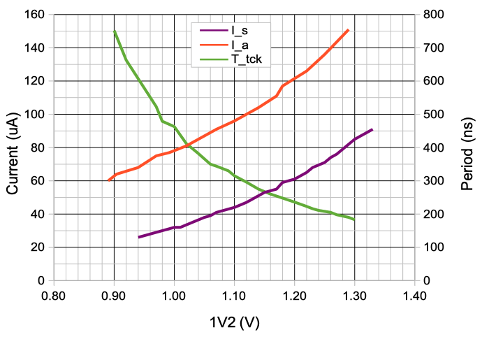
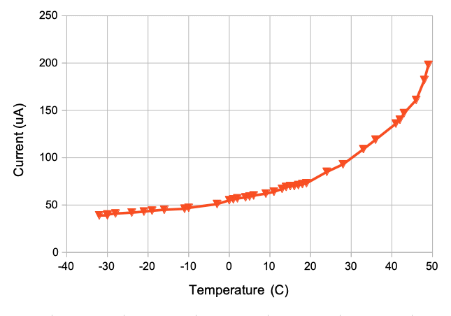
The static current consumption of our logic is the current it consumes when it is doing absolutely nothing: no clock is running, no code is being executed, not gates are transitioning from one state to another. The static current consumption of an XO2-ZE devices is a strong function of its core power supply voltage. We call this voltage "1V2" in our circuit diagrams, named after its nominal value for the XO2-ZE devices. The X02 family data sheet specifies a recommended range for 1V2 of 1.14 V to 1.26 V, with an absolute maximum of 1.32 V. We lowered 1V2 from 1.30 V to 0.94 V in steps at 20°C and saw the static current consumption of an LCMXO2-1200ZE drop from 85 μA to 26 μA. The speed of the device is also strong function of 1V2. When our TCK ring oscillator generates 5 MHz with 1V2 = 1.26 V, the same oscillator runs at onlyu 1.7 MHz with 1V2 = 0.94 V. In order to power up the device successfully, however, we find empirically that we need 1V2 ≥ 1.10 V. In our A3051 Blood Pressure Monitor, we start with 1V2 = 1.20 V and later drop 1V2 to 1.02 V using a particular buck converter, the ST1PS02A, which provides digital voltage adjustment. By calibrating our ring oscillator at this lower voltage, we set TCK to 5 MHz for 1V2 = 1.02 V, and so are able to take advantage of the reduced quiescent current at this lower voltage. The OSR8 microprocessor, which is guaranteed to run at 8 MHz for 1V2 ≥ 1.14 V, runs reliably at 5 MHz even with 1V2 = 1.02 V.
The static current consumption of the XO2-ZE devices increases rapidly with temperature. We measured the static current consumption of the LCMZO2-1200ZE in a TQFP-100 package with 1V2 set to 1.23 V and found it to be 125 μA at 37°C and 75 μA at 20° C. Our implants must operate at 37°C, so it is the static current consumption at this temperature that we must use in our estimates of implant operating life. We will assume that the static current consumption at 37°C is 125 / 75 = 1.7 times the static current consumption at 20°C. Our static current consumption at 20°C and 1V2 = 1.02 V is 30 μA, so at 37°C we expect it to be 30 μA * 1.7 = 51 μA. Table 3.9 in the MachXO2 data sheet specifies typical static current consumption of 56 μA for the LCMXO2-1200ZE at 1V2 = 1.2 V and 25°C. Our observed static current consumption at 1V2 = 1.02 V and 37°C is 51 / 56 = 91% of the data sheet's typical value. Assuming this ratio holds for the other members of the XO2-ZE family, we expect the static current consumption of the LCMXO2-2000ZE at 1V2 = 1.02 V and 37°C to be 91% * 80 μA = 73 μA. This device, in the WLCSP-49 package, is another potential platform for an OSR8 in an implantable device.
Our implants are equipped with a 3.0-V power supply, such as provided by a one 3.0-V coin cell or two 1.5-V coin cells in series. We want to provide the LCMXO2-1200ZE logic with core power supply voltage 1V2 = 1.20 V at startup and afterwards drop 1V2 down to 1.02 V. In order to decrease the current drawn from the battery, we produce 1V2 with a buck converter. We use the ST1PS02A because it allows us to switch 1V2 from a nominal 1.20 V down to a nominal 1.00 V by applying a logic HI to one of its control pins. When our XO2-ZE device powers up, it drives this pin LO, and we see 1V2 = 1.21 V. Once it has completed its self-configuration and entered standby, it drives the pin HI and we see 1V2 drop to 1.02 V. The converter is 80% efficient at converting 3.0 V into 1.0 V, so the logic chip's static current consumption of 51 μA at 1.02 V and 37°C will draw only 51 * 1.02 / 3.00 / 80% = 22 μA from the battery. Referring once again to Table 3.9 in the MachXO2 data sheet, we see that this 22 μA drawn from the battery is 39% of the 56 μA typical static current consumption of the LCMXO2-1200ZE with 1V2 = 1.20 V at 25°C. Assuming this ratio holds for the other members of the XO2-ZE family, we expect the LCMXO2-2000ZE to draw 39% * 80 μA = 31 μA static current from our battery, given that its typical static current consumption at 1V2 = 1.20 V and 25°C is 80 μA.

The dynamic current consumption of the logic chip is the current consumed by logic transitions. When logic gates trasnsition from one state to another, parasitic capacitors must be charged and discharged. These capacitors do not change much with temperature, and as a result, the dynamic current consumption does not change much with temperature either. The dynamic current consumption does, however, change with the core logic power supply voltage, which we call 1V2 for XO2-ZE devices. The amount of charge required to bring about a logic level transition is proportional to the voltage change on the parasitic capacitors. We measured the dynamic current consumption of the LCMXO2-1200ZE on our A3051 Blood Pressure Monitor by subtracting its static current from its active current. We observed dynamic current consumption 50 μA at 1V2 = 1.00 V and 60 μA at 1V2 = 1.20 V, which is consistent with exact proportionality between dynamic current and power supply voltage. Thus we assume that the dynamic current consumption of our OSR8 will be proportional to its core logic power supply voltage.
We now consider how we might estimate the dynamic current consumption of an OSR8-equipped LCMXO2 device. We use as our guide an experiment we performed with our A3041 Implantable Stimulator-Transponder. This device hosts an OSR8 and several substantial state machines in an LCMXO2-1200ZE with 1V2 = 1.23 V. With the TCK ring oscillator enabled and running at 5.0 MHz and the OSR8 running at 32.768 kHz, dynamic current consumption was 800 μA. When we switched the OSR8 to run on TCK = 5.0 MHz, dynamic current consumption increased from 800 μA to 1.9 mA. From this we conclude that the dynamic current consumption of the OSR8 alone is 1.1 mA at 5 MHz, or 220 μA/MHz when we have 1V2 = 1.23 V. At our preferred 1V2 = 1.02 V, we expect the dynamic current consumption of the OSR8 to be 1.02 / 1.23 * 1.1 mA = 900 μA at 5-MHz, or 180 μA/MHz.
Our Transmit Clock (TCK) ring oscillator has the great avantage of being able to turn on and off immediately. In the A3041 Implantable Stimulator-Transponder firmware, we use the Interrupt Service (ISRV) output from the OSR8 to turn on TCK and put the CPU in boost mode within 200 ns, and later to move it out again at the end of the interrupt within a few microseconds. Our study of the OSR8 deployment in the A3041 showed that the TCK clock generator consumed 800 μA at 1V2 = 1.23 V. The generator in the A3041 consisted at that time of a ring oscillator with four gates running at 130 MHz, and a divider that produced 5 MHz for TCK. This is the equivalent of 5 gates running at 130 MHz, or 1 gate running at 650 MHz. The LCMXO2-1200ZE dynamic current consumption for a single gate is around 800 μA / 650 MHz = 1.2 μA/MHz with 1V2 = 1.23 V. If we drop 1V2 down to our preferred 1.02 V, two effects come into play: the dynamic current consumption decreases in proportion to the power supply voltage, and the speed of the gates decreases as well. With 1V2 = 1.02 V, our ring oscillators run at 46% of their frequency at 1V2 = 1.02 V. We can still generate TCK = 5.0 MHz from the slower ring oscillator: we just divide it by a lower interger. Combining these two effects, the 1V2 current required to produce TCK = 5.0 MHz with 1V2 = 1.02 V is only 800 μA * 46% * 1.02 V / 1.23 V = 300 μA. Considering the current consumption of just one gat switching at 1 MHz, its current consumption will be 1.2 μA/MHz * 1.02 V / 1.23 V = 1.00 μA/MHz, and from the battery it will draw 1.00 μ * 46% = 460 nA/MHz.
Given that our the OSR8 running its main loop at 1V2 = 1.23 V consumes 220 μA/MHz, and a single gate running at 1 MHz at the same voltage consumes 1.2 μA/MHz, we conclude the activity generated by our main loop in the logic chip is equivalent to 180 μA / 1.2 μA/MHz = 150 gates. When estimating the OSR8 dynamic current consumption in any logic chip, we can take the dynamic consumption of one gate at the clock frequency and multiply by 150 to get the current consumption of the processor.
Combining the above calculations, we can estimate the current consumption of the OSR8 hosted in an LCMXO2-1200ZE. We assume our core power supply voltage 1V2 = 1.02 V and operating temperature is 37°C. Under these conditions, the static current consumption of the LCMXO2 is 51 μA. When we turn on the 5-MHz oscillator, the oscillator consumes 300 μA. When we run actice code on the OSR8 at 5 MHz, the OSR8 consumes an additional 900 μA. When running active code at 32.768 kHz, the OSR8 consumes an additional 6 μA. In slow mode, with the 5-MHz oscillator turned off and the OSR8 running on 32.768 kHz, the logic chip consumes 51 μA + 6 μA = 57 μA. In boost mode, with the OSR8 running off the 5-MHz oscillator, the logic chip consumes The OSR8 consumes 51 μA + 300 μA + 900 μA = 1251 μA. If we are providing 1V2 = 1.02 V from a 3-V battery with an 80% efficient buck converter, the logic chip will draw 24 μA in slow mode and 530 μA in boost mode.
[13-FEB-26] The maximum clock speed with which we can drive the OSR8 depends upon the manner in which the logic functions are distributed and the underlying speed of the logic chip in which the OSR8 is deployed. When we compile the OSR8 and accompanying peripheral state machines and management processes into an LCMXO2-1200ZE, we tell the compiler to minimize area, not maximize speed. If we don't specify area minimization, the design does not fit in the available 1280 LUTs. As it is, the Implantable Stimulator-Transponder (IST) firmware occupies 1244 LUTs. The Lattice Diamond timing analyzer assumes, by default, a core supply voltage of 1.14 V and junction temperature 100°C. Under these conditions, the analyzer gives a maximum OSR8 clock speed of 8.2 MHz. If we drop the temperature to 37°C, the maximum clock speed drops to 8.1 MHz. At 1.23 V and 37°C, the maximum clock speed is 10.2 MHz. The compiler will not let us specify a core power supply voltage lower than 1.14 V, but our implants run at 1.02 V. Assuming linearity, we get a slope of 23 kHz/mV for clock speed versus power supply voltage. At 1.02 V we expect to be able to run at 5.34 MHz. We run our implanted OSR8s at 5.0 MHz.
The same Lattice Diamond timing analysis tells us that OSR8 transitions must pass through "10 levels" before they settle. Each "level" consists of a LUT, possibly a register, and a path by which the output will be distributed to its destinations. We know the single-gate propagation delay of the LCMXO2-1200ZE from the frequency of our four-gate ring oscillator, which is 130 MHz at 1V2 = 1.23 V. We take this 7.5-ns period and divide by two to get the time it takes a transition to pass through four gates, and then by four to get the delay through one gate, and so obtain 0.9 ns as the single-gate delay. The timing analyzer itself specifies a gate delay of 0.92 ns. The maximum clock frequency for our OSR8 at 1V2 = 1.23 V is 10.2 MHz, for period 98 ns. The OSR8 uses both edges of the clock, so some signals must settle in a half-period, or 49 ns. Others have 98 ns to settle, because they are not needed until the next edge. The text below is an example path timing report. We see the ten levels, and how the total delay is broken down between gates and routes. The look-up of a byte from program memory is the first thing in the path, and takes 10.2 ns, followed by another 9.5 ns for the byte to reach the CPU. Subsequent routing is anything from 0 ns, when the two signals are in the same LUT, to 7.7 ns, when they are distant.
Constraint Details:

     60.027ns physical path delay ROM/ROM_0_0_3_0 to CPU/SLICE_126 meets
    100.000ns delay constraint less
      0.273ns skew and
      0.430ns DIN_SET requirement (totaling 99.297ns) by 39.270ns

 Physical Path Details:

      Data path ROM/ROM_0_0_3_0 to CPU/SLICE_126:

   Name    Fanout   Delay (ns)          Site               Resource
C2Q_DEL     ---    10.197 EBR_R6C20.CLKB to EBR_R6C20.DOB0 ROM/ROM_0_0_3_0 (from CK)
ROUTE        19     9.523 EBR_R6C20.DOB0 to R5C10D.B0      prog_data[6]
CTOF_DEL    ---     0.920      R5C10D.B0 to      R5C10D.F0 CPU/SLICE_431
ROUTE        10     5.405      R5C10D.F0 to R3C18A.A1      CPU/N_765
CTOF_DEL    ---     0.920      R3C18A.A1 to      R3C18A.F1 CPU/SLICE_470
ROUTE         8     2.477      R3C18A.F1 to R4C19D.D1      CPU/N_759
CTOF_DEL    ---     0.920      R4C19D.D1 to      R4C19D.F1 CPU/SLICE_451
ROUTE         2     3.531      R4C19D.F1 to R8C21A.C1      CPU/alu_in_x_iv_1[3]
CTOF_DEL    ---     0.920      R8C21A.C1 to      R8C21A.F1 CPU/SLICE_353
ROUTE         2     4.106      R8C21A.F1 to R3C20C.B0      CPU/alu_in_x_iv_3[3]
C0TOFCO_DE  ---     2.057      R3C20C.B0 to     R3C20C.FCO CPU/SLICE_3
ROUTE         1     0.000     R3C20C.FCO to R3C20D.FCI     CPU/un1_alu_in_x_cry_4
FCITOF1_DE  ---     1.294     R3C20D.FCI to      R3C20D.F1 CPU/SLICE_2
ROUTE         1     2.922      R3C20D.F1 to R4C21A.A1      CPU/un1_alu_in_x_cry_5_0_S1
CTOOFX_DEL  ---     1.354      R4C21A.A1 to    R4C21A.OFX0 CPU/result_1[6]/SLICE_312
ROUTE         5     7.673    R4C21A.OFX0 to R7C21A.D1      CPU/alu_out[6]
CTOF_DEL    ---     0.920      R7C21A.D1 to      R7C21A.F1 CPU/SLICE_350
ROUTE         1     3.968      R7C21A.F1 to R4C15B.A0      CPU/next_flag_z_2_m_6
CTOF_DEL    ---     0.920      R4C15B.A0 to      R4C15B.F0 CPU/SLICE_126
ROUTE         1     0.000      R4C15B.F0 to R4C15B.DI0     CPU/next_flag_z_8 (to CK)
                  --------
                   60.027   (34.0% logic, 66.0% route), 10 logic levels.
The Animal Location Tracker (ALT) firmware resides in an LCMXO2-7000HC, which we power with 3.3 V, which it regulates to 1.2 V internally. This device provides 6864 LUTs. Here we have no worries about space. We compile to maximize speed. The HC devices have an internal regulator to produce the core supply. If we set this core voltage to 1.2 V, the OSR8 maximized for speed will run at 22 MHz. We run it at 20 MHz.
[16-FEB-26] For design and development of the OSR8, see its Design Page.