| Description |
| Versions |
| Set-Up |
| Stimulus Current |
| Battery Life |
| Heating |
| Operation |
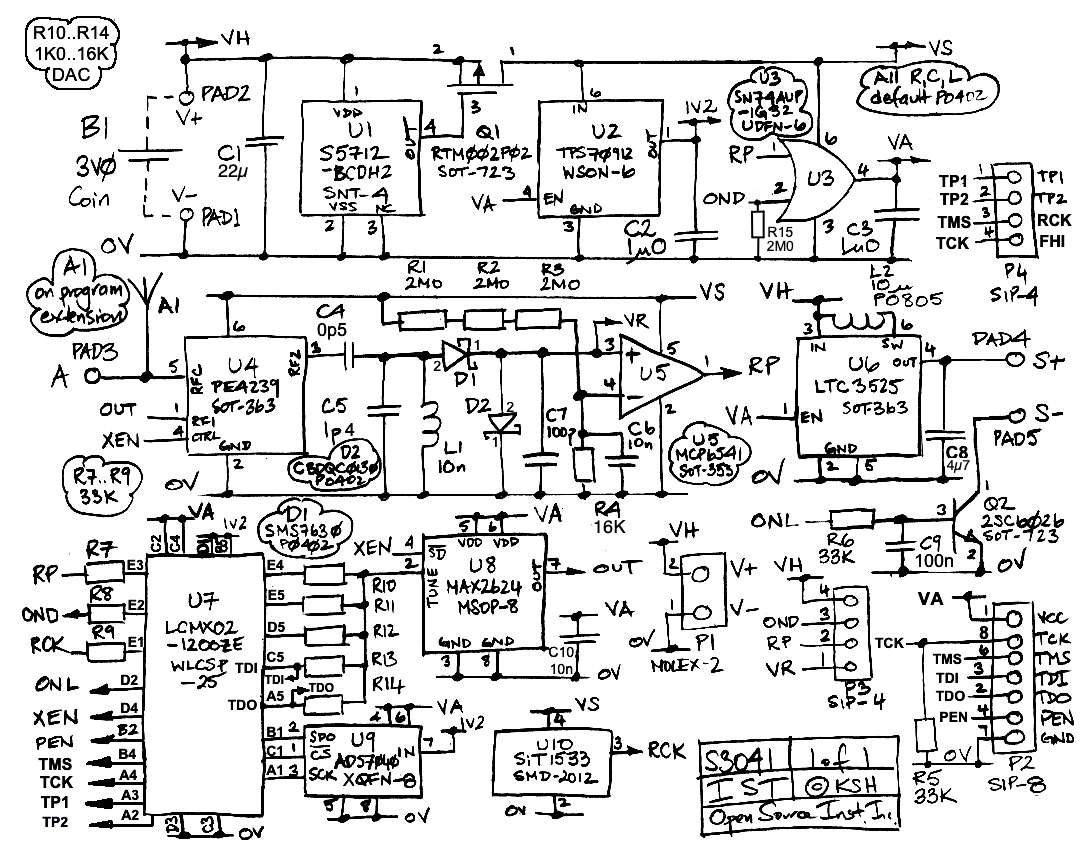
| Design |
[11-MAY-26] The A3041 Implantable Stimulator-Transponder (IST) receives commands through its crystal radio, interprets these commands and executes them with its own embedded microprocessor, applies stimuli to its two stimulus leads, transmits a synchronizing telemetry signal upon command, and reports its own battery voltage. We ship the A3041 with a magnet attached. The magnet that keeps it in its sleep state, which minimises its current consumption. When we remove the magnet, the A3041 enters its wake state. When the A3041 receives a command, it becomes active. If instructed to do so, the A3041 will generate a stimulus consisting of electrical pulses of current applied to its stimulation leads. The magnitude of the current, the duration of the pulses, their period, their quantity, as well as whether they should be regular or random, are all specified in a single command. By uploading user-programs through its crystal radio and into the memory of its microprocessor, we can configure the A3041 to provide arbitrarily complex stimuli that suit our own experiment.

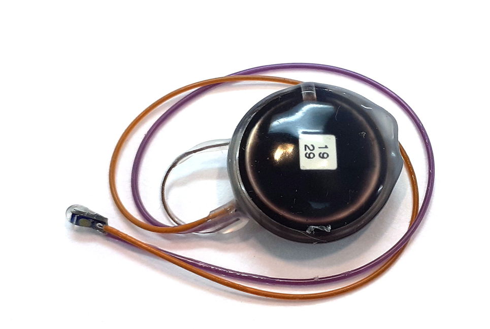
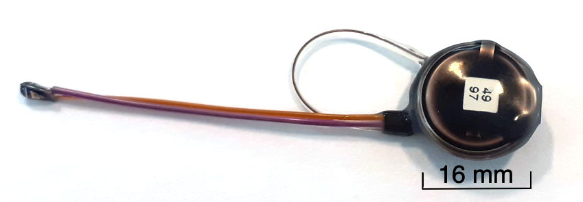
The A3041 Implantable Stimulator-Transponder is equipped with two flexible leads that carry its stimulus current to the stimulus site. At the end of each lead is a pin. The two pins will mate with the sockets on an Implantable Light-Emitting Diodes (ILED), or they can mate with two sockets on a bipolar depth electrode. The A3041 drives its stimulus leads with a current source. We set the magnitude of the current with a code that we transmit to the stimulator. The current source is unidirectional: current flows out of the L+ pin on the end of the orange lead and into the L− pin on the end of the purple lead. The A3041 cannot be used for alternating current stimulation, only for pulsed direct current stimulation. The A3041A34 versions provide currents from 200 μA to 10 mA with a maximum applied voltage of 3.3 V. The A3041F55 provides currents 600 μA to 30 mA with a maximum applied voltage of 5.0 V. The table below provides a full specification for one particular version.
| Property | Value |
|---|---|
| Volume of Implant | 1.1 ml |
| Mass of Implant | 2.1 g |
| Battery Type | LIR1040 |
| Nominal Battery Capacity | 45 mA·hr |
| Stimulus Cost | 1.7 mA·hr/mA·hr |
| Active Life | 165 hr |
| Sleep Current | 2.2 μA |
| Sleep Control | sleeps in magnetic field |
| Wake Current | 5.5 μA |
| Active Current | 140 μA @ 37°C |
| Stimulus Voltage | 5.0 V |
| Stimulus Current Range | 600 μA to 30 mA |
| Pulse Length Range | 2 ms to 60 s |
| Pulse Period Range | 4 ms to 60 s |
| Stimulus Length Range | 1 to 60k pulses |
| Operating Range | 30 cm |
| Lead Dimensions | 45 mm long × 0.7 mm dia |
| Lead Terminations | Soldered D-Pins |
| Total Lead Resistance | 56 Ω |
| Antenna Dimensions | 30-mm thin stranded loop |
The A3041 Implantable Stimulator-Transponder uses its antenna to receive wireless commands and to transmit wireless messages. The operating range of the IST is the range from its nearest command antenna for which reception of commands is ≥95%. We transmit commands to an IST with a command transmitter such as an A3042B Telemetry Control Box, which provides both telemetry reception for telemetry sensors and command transmission for implanted stimulators. We control the command transmitter with the Stimulator Tool in our LWDAQ software. The IST can transmit acknowledgements, its version number, and battery measurements. It can identify itself in response to a multicast request. It will transmit a synchronizing signal that shows when its stimulus pulses occur. When the A3041 transmits its synchronizing signal, it uses a telemetry channel that we assign in the transmit command. All A3041 transmissions use our SCT telemetry system protocol. The commands they receive from the command transmitter use the same radio frequency, but a different protocol. The commands consist of slow, high-power pulses, while the transmissions consist of micropower, frequency-modulated bursts.
In addition to its buit-in stimulator function, the A3041 Implantable Stimulator-Transponder allows us to upload our own programs to run on its embedded OSR8 microprocessor. These programs, written in the OSR8 assembly language, can be up to 2 KBytes long. By means of the user programs we can provide new and complex stimuli as required by particular experiments. See the Stimulator Tool manual for details of how to prepare and upload programs to the A3041 memory. The A3041's user program memory is volatile, so all programs are lost when the device deactivates into its wake or sleep states.
[29-APR-26] The table below lists the A3041 Implantable Stimulator-Transponder configuration options. The battery type dictates the A3041's battery capacity and mass. To drive the highest currents through the longest leads, we need a 5-V stimulus voltage. Electrical stimulation can be better controlled with a range of currents up to 300 μA. On the other extreme, optogenetic induction of spreading depolarization can require currents up to 30 mA. The A3041 can be configured for five different current ranges to accommodate diverse applications. Otherwise, we use 3.3 V for the stimulus, which consumes less current from our battery for each milliamp stimulus current. In rats, we need the leads to be around 130 mm, while in mice they can be as short as 35 mm. The lower the resistance of the leads, the thicker and less flexible the lead will be. A longer antenna is good for implantation in rats, a shorter one for mice.
| Option | Unit | Choices |
|---|---|---|
| Battery | Type | CR1220 (A), LIR1040 (B), LIR1620 (C), LIR1254 (D), LIR2032(F) |
| Stimulus Voltage | V | 3.3 (3), 5.0 (5) |
| Stimulus Current Range | mA | 0.006-0.3 (1), 0.02-1 (2), 0.06-3 (3), 0.2-10 (4), 0.6-30 (5) |
| Lead Length | mm | 30 mm to 260 mm |
| Lead Resistance | Ω/cm | 1.6 (D), 6.3 (B), 25 (C) |
| Antenna Length | mm | 30 (D), 50 (E) |
The table below lists a selection of possible A3041 Implantable Stimulator-Transponder version from lightest to heaviest. Each version has its own unique part number beginning with "A3041", followed by one or two letters specifying the battery, a digit specifying the stimulus voltage, and another digit specifying the maximum stimulus current. The battery letter codes are defined by the table itself. The length, type, and termination of the stimulus leads, as well as the antenna type, are further configuration options that complete the part number of a particular A3041 device.
| Version | Battery Type |
Battery Capacity (mA·hr) |
Max Voltage (V) |
Current Range(mA) |
Stimulus Cost (mA·hr/mA·hr) |
Active Life (hr) |
Wake Life (wk) |
Shelf Life (wk) |
Volume (ml) |
Mass (g) |
|---|---|---|---|---|---|---|---|---|---|---|
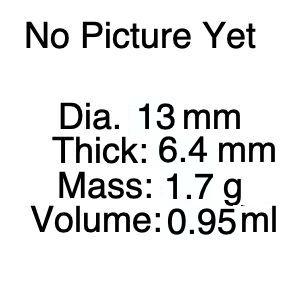
| A3041A34 | CR1220 | 30 | 3.3 | 0.2—10 | 1.5 | 150 | 30 | 9 | 0.95 | 1.7 |
| A3041B34 | LIR1040 | 35 | 3.3 | 0.2—10 | 1.1 | 175 | 35 | 10 | 1.1 | 2.1 |
| A3041B55 | LIR1040 | 35 | 5.0 | 0.6—30 | 1.7 | 175 | 35 | 10 | 1.1 | 2.1 |
| A3041D34 | LIR1254 | 65 | 3.3 | 0.2—10 | 1.1 | 325 | 65 | 20 | 1.6 | 3.1 |
| A3041F55 | LIR2032H | 70 | 5.0 | 0.6—30 | 1.7 | 350 | 70 | 21 | 2.7 | 4.8 |
| A3041C55 | LIR1655 | 110 | 5.0 | 0.6—30 | 1.7 | 550 | 110 | 33 | 3.0 | 5.4 |
We specify the lifetime of the A3041 Implantable Stimulator-Transponder in four distinct states: sleeping, waking, delivering a high-power stimulus, and delivering a low-power stimulus. All versions of the A3041 sleep when they are in contact with a magnet, which is how we store A3041s on the shelf. It's shelf life is how long it can sleep before and still have 90% of its battery capacity remaining. An A3041 wakes up when we keep it away from any magnet. When awake, the A3041's crystal radio is powered up and ready to receive commands. It's wake life is how long it can remain awake when starting with a fresh battery. An A3041 Implantable Stimulator-Transponder activates when it receives a command. When active, its logic chip and stimulation voltage are powered up and consuming current. The active life is the minimum length of time the A3041 can remain in its active state while implanted and when starting with a fresh battery. The active life applies to stimuli that use hardly any power, such as 10 ms pulses of 200 μA at 10 Hz, and perhaps transmitting a synchronizing signal as well so that our telemetry system can see when the pulses occur. When we are delivering a significant stimulus current, we must account for the drain on the battery that is due to the stimulus current alone. The stimulus cost is the number of milliamp-hours of battery capacity that is consumed for each milliamp-hour of charge delivered to the stimulus site. The stimulus cost is independent of the stimulus cost and stimulus duty cycle, except when we are using one of the A3041A-series stimulators. The A3041A-series devices are not designed for continuous, high-current stimuli. The stimulus cost we specify for the A3041A34 is valid only if we deliver maximum current for no more than 100 ms, and provided the average stimulus current is no greater than 1 mA.
We equip the A3041 Implantable Stimulator-Transponder with our flexible leads. By default, we use orange and purple B-Leads. These are 0.7 mm in diameter, contain a spring of stainless steel wire 450-μm in diameter, and present resistance 6.3 Ω/cm. These leads can be anything from 30 mm to 280 mm long. The other lead options are the much more flexible C-Leads, which are 0.5 mm in diameter, contain a 250-μm spring, and present resistance 25 Ω/cm, and the much heavier D-Leads, which are 0.8 mm in diameter, contain a 500-μm diameter spring, but present a resistance of only 1.6 Ω/cm. At the ends of the leads, we can have bares wire for delivering electrical stimulation, or pins to connect to depth electrodes or an A3036IL Implantable Light-Emitting Diode (ILED). See our Catalog of Electrodes and our A3036IL Manual for more details.
[16-APR-26] We transmit commands to the A3041 Implantable Stimulator-Transponders and receive its acknowledgements, battery voltage measurements, and synchronizing signals with with a Telemetry Control Box (TCB), such as the A3042B-16 Sixteen-Antenna TCB. Each A3042-B antenna acts as both a telemetry receiver and a command transmitter. We control the transmission of commands and manage the reception of acknowledgements and battery voltage measurements using the Stimulator Tool, which is included in our LWDAQ Software.
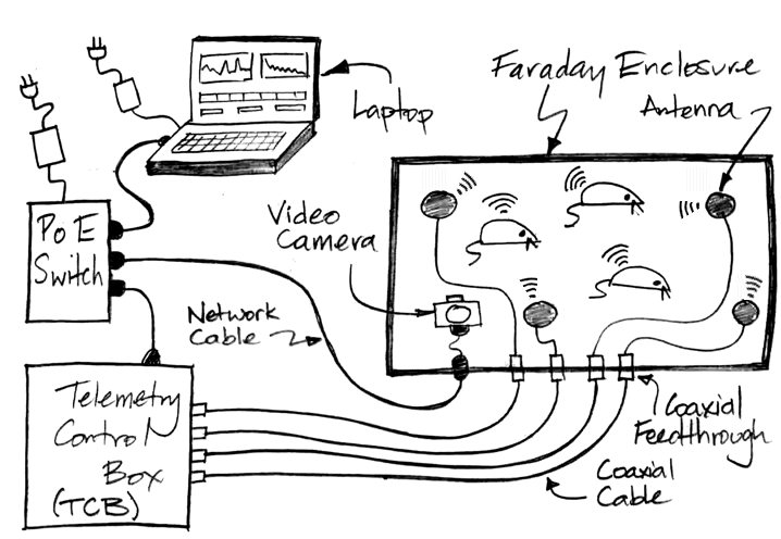
All A3042 Telemetry Control Boxes receive their power from the PoE connection, and all communication with an A3042 takes place over the same PoE cable. The burst of power required to transmit on sixteen antennas comes from an internal lithium-polymer battery that recharges in the minutes after command transmission. If our experiment requires stimuli that cannot be defined simply with a pulse period, pulse length, stimulus current, and stimulus duration, we can upload a custom stimulus definition to an A3041 Implantable Stimulator-Transponder with the help of the Stimulator Tool. The custom instructions must be written in the assembler language of the A3041's embedded OSR8 microprocessor and converted into a hexadecimal string by our the LWDAQ software's built-in OSR8 assembler.
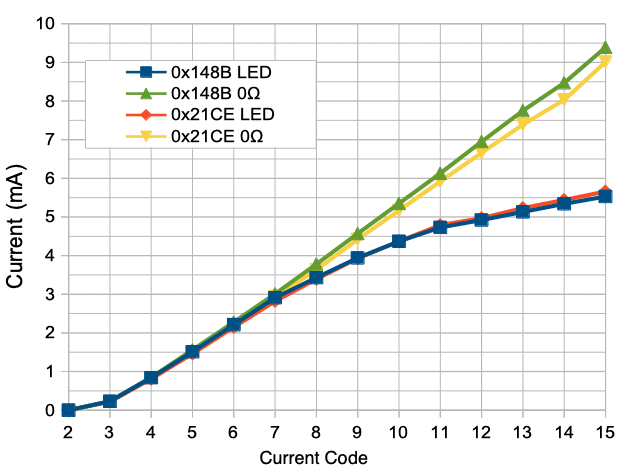
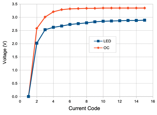
[16-APR-26] The A3041's stimulus output is limited in both current and voltage: there is a maximum voltage it will apply to the stimulus leads and a maximum current it will allow to flow through the stimulus leads. The maximum voltage is a function of the boost converter we load onto the A3041 circuit. It can be 3.3 V or 5.0 V. In the case of the A3041A34, the maximum voltage is 3.3 V. The current is controlled by a four-bit current code we select in Stimulator Tool. Its value can be 0-15. The magnitude of the current is inversely proportional to the value of a resistor on the circuit (See R6 S3041A_1). In the A3041A34, the maximum current is 10 mA, while the minimum is a little over 200 μA. In all versions, the minimum is roughly 2% of the maximum.
Each A3041 Implantable Stimulator-Transponder has a maximum voltage that its stimulus current source can apply to the base of its stimulus leads. This maximum is either 3.3 V or 5.0 V depending upon the A3041 version. This maximum cannot be changed by a command, it is a permanent feature of any given A3041 circuit. The A3041A34 is capable of delivering up to 10 mA to a load, but only if 3.3 V is sufficient to drive 10 mA through the load. If the stimulator's leads have combined resistance 50 Ω and we have a green LED at the end with forward voltage 2.8 V at current 10 mA, our load requires exactly 3.3 V, and we should be able to get 10 mA to flow through the LED. But if our lead resistance is 100 Ω, we will instruct the stimulator to deliver 10 mA and find that it delivers only 5 mA.
If we want to deliver 10 mA to an ILED at the end of 130-mm leads, the resistance of the leads becomes significant. At 30 mA, the resistance of the leads is critical and requires that we use a stimulator with a 5-V stimulus voltage. If we use B-Leads, we have a total of 26 cm of 0.7-mm diameter B-Lead, so total resistance is 26 * 6.3 Ω/cm = 164 Ω. A 10-mA current will drop 50 Ω * 10 mA = 1.6 V in the leads. If we combine this with a blue LED that needs 2.9 V forward voltage at 10 mA, we need a total voltage of 1.6 + 2.9 = 4.5 V. We must use a 5-V version of the A3041. Another option is to use a 3.3-V version, but equip the stimulator with the low-resistance D-Lead instead. The D-Lead is made with thicker wire and wound with fewer coils per unit length. It is less flexible than the B-Lead, but its resistance is only 1.6 Ω/cm. At length 130 mm, two D-Leads combined have resistance 26 cm * 1.6 Ω/cm = 42 Ω, so a 3.3-V stimulator is sufficient. Our stimulus cost will decrease if we use a lower stimulus voltage, so we extend the operating life of our stimulator by using lower-resistance leads and a lower stimulus voltage. If we want to drive 30 mA through a blue LED, the voltage across the LED increases to 3.2 V and the voltage required by the leads increases to 42 Ω * 30 mA = 1.3 V. We need at least 4.5 V, so we must choose a 5-V stimulator.
[26-JUN-26] We want be able to estimate before-hand whether or not an A3041 Implantable Stimulator-Transponder has sufficient battery life to complete any given experiment. Because the stimulator can be in a variety of states, and provide a wide range of stimuli, we must calculate separately the battery capacity it consumes in each of these states, and we must repeat this calculation for each new experimental protocol. Each stimulator battery has a nominal capacity, which is the amount of electrical charge it can deliver before it is exhausted. We express battery capacity in milliamp-hours (mA·hr). Each milliamp-hour provides us with a certain amount of time in the sleep state, wake state, and active state. One milliamp-hour of battery current provide us with a certain number of milliamp-hours of stimulus current. But we usually look at these values the other way around: one week of sleep uses a certain amount of battery capacity, one milliamp-hour of stimulus current uses a certain amount of battery capacity, and so on, until we have added together the charge consumption of all parts of our experimental protocol and arrive at a total requirement in milliamp-hours that we must then hope is less than the actual battery capacity of our stimulators.
| State | Consumption Rule |
|---|---|
| Sleep (disabled by magnet, sitting on shelf) | 0.33 mA·hr/wk |
| Wake (enabled and awaiting commands) | 1.0 mA·hr/wk |
| Active (average stimulus current ≤30 μA) | 0.20 mA·hr/hr |
| Stimulus Cost (average stimulus current >30 μA) | S mA·hr/mA·hr |
The device is asleep when sitting on its magnet. We use 0.33 mA·hr for each week the stimulator spends in its sleep state. The device is awake when it has been removed from its magnet and is doing nothing except for waiting for commands. We use 1.0 mA·hr for each week the stimulator spends in its wake state. The device is active when it is powered up and delivering a low-power stimulus or transmitting a synchronizing signal. We use 0.20 mA·hr for each hour we spend in the active state. When the device is delivering a significant current to its stimulus leads, we calculate the charge drawn from the battery by multiplying the stimulus charge by the stimulator's stimulus cost. The stimulus cost is given for each stimulator in the A3041 Version Table. In the case of the A3041A34, which is equipped with a CR1220 battery, the stimulus cost is correct only if we avoid damaging the battery with continuous, high-current stimuli. If we turn on the maximum stimulus current continuously, we must do so for no more than 100 ms and no more than for no more than 10% of the time. In all other A3041s, which are equipped with LIR-series batteries, there is no restriction on the length or frequency of the stimulus. The stimulus current cost for these stimulators is the same for all currents and pulse durations.
Example: We propose to implant A3041A34s in mice, administer an average of twelve stimuli per day, each stimulus being 10-ms pulses of 10 mA at 10 Hz applied to an implantable lamp for one minute. We want the study to continue for at least eight weeks. Our A3041A34s have been sitting on the shelf for 9 weeks with their magnets attached, hibernating. The hibernation used 3 mA·hr. During our experiment, the stimulators will be awake for eight weeks, which uses 8 mA·hr. Each stimulus is 10 ms * 10 Hz * 60 s * 10 mA = 60 mA·s. We want each stimulator to deliver twelve stimuli per day for at least eight weeks, so the stimuli will use 12 * 8 * 7 * 60 mA·s = 11 mA·hr of stimulus charge. The active current of the stimulator is negligible compared to the stimulus current cost, so we will ignore the active current. The A3041A34's stimulus current cost is 1.5 mA·hr/mA·hr, so our stimulus takes 17 mA·hr. Our total use is 3 + 8 + 17 = 28 mA·hr. The A3041A34 battery capacity is 40 mA·hr. We have 12 mA·hr of capacity to spare.
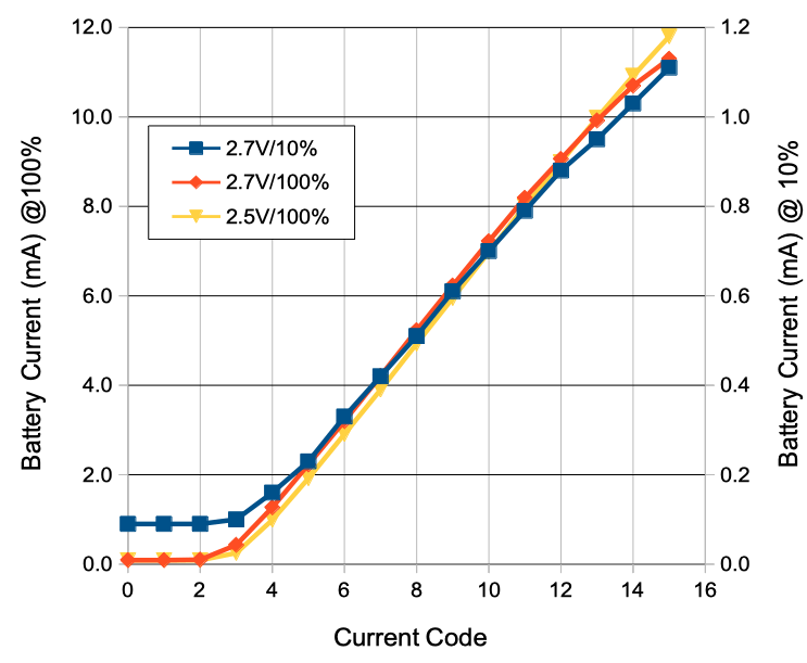
All our A3041 Implantable Stimulator-Transponders are equipped with coin cell batteries. The A3041A34 is the smallest. It is equipped with a CR1220 battery that imposes some limits on the length of maximum current pulses. But all the others are powered by LIR-series batteries that can provide their maximum current continuously with ease. The voltage produced by CR-series batteries is 3.0 V for most of the battery's life, provided we measure the voltage during a low-power stimulus. When down to 5% capacity, the voltage will drop to around 2.7 V. The voltage of LIR-series batteries is 3.8 V when it is at 95% capacity and drops to 3.6 V when is is at 5% capacity, so we can get a good idea of where we are in an LIR-series battery's life by looking at the A3041's report of its voltage. When we calculate the stimulus current cost of a stimulator, we use 3.7 V as the battery voltage for LIR-series batteries and 2.7 V for CR-series batteries. Regardless of the battery type, when an A3041's battery voltage drops below 2.4 V, even for a moment, the A3041 circuit will shut down and return to its wake state.
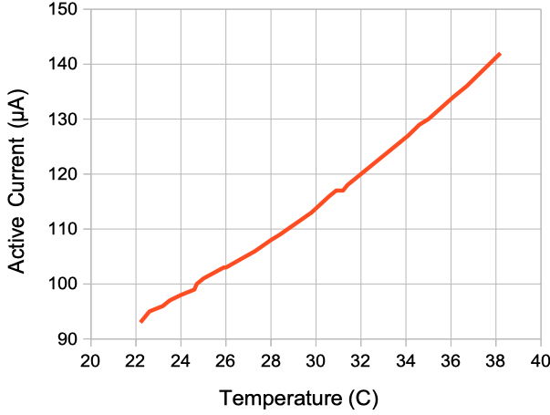
In its sleep state, the A3041 Implantable Stimulator-Transponder consumes 2.0 μA. Without a magnet, the A3041 is awake until it receives a command. While awake, the A3041 consumes 5.5 μA. When it receives a command, it activates, and remains active until it has completed all instructions. The A3041's current consumption increases with stimulation current, pulse length, pulse frequency, synchronizing signal rate, and randomization. The cost of generating timing signals for pulses is 0.28 μA/PPS (microamp per pulse per second). The additional cost of randomizing the production of these pulses is 0.86 μA/PPS. The cost of synchronizing transmission is 0.22 μA/SPS (microamp per sample per second). Furthermore, the active current increases with temperature, see here. To account for this increase, we add a temperature-dependent correction to the active current. At 37°C, an active A3041 consumes roughly 40 μA more than it does at 25°C. In order to simplify our battery life calculations, we just assume that an active, implanted A3041 consumes 200 μA from its battery when it is providing a low-power stimulus. We it is delivering a high-power stimulus, we add the cost of the stimulus current to the active cost to obtain our total current consumption.
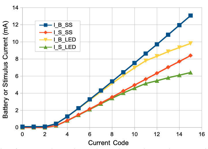
As we increase the current code, our stimulus current increases. As the stimulus current increases, so does the battery current. If our stimulus operates on a 10% duty cycle, the battery current drawn by the stimulus will be almost ten times smaller.
The current drawn from the battery, IB, is different from our stimulus current, IS, because the stimulus current is produced from the battery voltage by an inductive converter circuit. When the battery voltage, VB, is less than the stimulus voltage, VS, the battery current will be greater. When the battery voltage is less than the stimulus voltage, the battery current will be less. The converter efficiency, η, is approximately 80%. The battery current will be IB = VS / VB * IS / η. But it is not easy to know what the battery voltage will be during a stimulus pulse. In the case of the A3041A34, with its CR1220 battery, the battery voltage drops to about 2.7 V during stimuli, so we estimate that IB = 3.3 / 2.7 * 1 mA / 0.80 = 1.52 mA. We assume that the battery current is 1.5 times the stimulus current for the A3041A34, so that the stimulus current cost is 1.5 mA·hr/mA·hr.
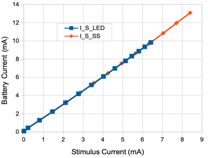
In the case of A3041 Implantable Stimulator-Transponders with LIR-series batteries, the battery voltage does not drop much during a stimulus, but it does drop during the life of the stimulator: from about 3.8 V to start with to 3.6 V when near exhaustion. We obtain our estimate of battery current by assuming battery voltage VB = 3.7 V and converter efficiency η = 80%. The A3041F55 has stimulus voltage VS = 5.0 V and maximum stimulus current IS = 30 mA. The battery current at maximum stimulus current will be 5.0 / 3.7 * 30 mA / 0.80 = 51 mA. The A3041F55's LIR2032 battery is specified for continuous current drain up to 70 mA. We assume the battery current is 1.7 times the stimulus current for all A3041s that provide a 5-V stimulus voltage from an LIR-series battery. Those that supply a 3.3-V stimulus voltage from an LIR-series battery draw 1.1 mA from the battery for each 1.0 mA of stimulus current.
[11-MAY-26] All but the smallest of our A3041 Implantable Stimulator-Transponders, when connected to an A3036 Implantable Light Emitting Diode (ILED), are capable of overheating the brain. For a discussion of heat generation by ILEDs and its rate of dissipation in the brain, see the Heating chapter of our Implantable Stimulator Overview.
[18-MAR-26] The A3041 functions are built around an OSR8 microprocessor. The firmware and software running in its logic chip are contained in a single GitHub repository P3041. The main program is ROM.asm. Through its crystal radio, the A3041 receives commands in the form of strings of instructions. Each instruction consists of an operation code, one or more operands, and one or more data bytes. The table below describes the instructions in detail.
| Opcode | Pneumonic | Name | Operands | Description |
|---|---|---|---|---|
| 0 | op_stop | Stimulus Stop | 0 | Stops the main program stimulus. |
| 1 | op_start | Stimulus Start | 8 | Defines and starts a main program stimulus. |
| 2 | op_xon | Synchronizing Signal | 2 | Start sync signal with frequency and channel. |
| 3 | op_off | Acknowledgement | 1 | Transmit acknowledgement with key. |
| 4 | op_batt | Report Battery Voltage | 0 | Measure and transmit battery voltage. |
| 5 | op_id | Announce Identity | 0 | All stimulators self-identify. |
| 6 | op_pgld | Load Program | 1 | Load a block of user program bytes. |
| 7 | op_pgon | Run Program | 0 | Run the user program. |
| 8 | op_pgoff | Halt Program | 0 | Halt the user program. |
| 9 | op_pgrst | Reset Load Pointer | 0 | Reset user program load location. |
| 10 | op_shdn | Shutdown | 0 | Deactivated the device, forcing it into wake state. |
| 11 | op_ver | Report Version | 0 | Transmit version number. |
A command consists of two ID bytes to specify the A3041 Implantable Stimulator-Transponder. The identifier 0xFFFF is the multicast ID. All A3041s will respond. We use the multicast ID to get all A3041s to identify themselves. Following the ID are the opcodes and their operands and data bytes. Last of all comes a two-byte checksum. We can see these bytes being listed before transmission in the text window of the Stimulator Tool when we have the Verbose box checked.
The A3041 Implantable Stimulator-Transponder can provide stimuli in one of two ways: a main-program stimulus or a user-program stimulus. The main program stimulus is entirely defined with five parameters: pulse length, pulse interval, number of pulses, pulse current, and randomize flag. The user program stimulus is defined by an OSR8 assembly program we upload to the stimulator. This program is subject to three restrictions: it executes once every 5 ms, it must not take more than 4 ms to execute, and its program size cannot exceed 2 KByte. Aside from these restrictions, the user program can implement any stimulus behavior.
To upload a user program, we use the Stimulator Tool's transmit panel, as described in User Programs. We prepare our user program in a text file containing OSR8 assembler. When we press Run Program, Stimulator Tool uploads and runs our program. It resets the program load location with op_pgrst. It uploads the program in one or more chunks using the op_pgld instructions. This upload takes place at roughly 1 KByte/s. A 100-byte program will take a fraction of a second to upload. A 2-KByte program will take several seconds. Once the upload is complete, the Stimulator starts the program running with op_pgon.
It is easy to freeze the A3041 Implantable Stimulator-Transponder with a user program. We can upload a program with an infinite loop and the A3041 will remain active until its battery runs down. When stuck in a loop running a user program, the A3041 consumes roughly 1.5 mA. Once an A3041 has been frozen by a faulty user program, the only way to unfreeze it is to force it to go to sleep with a magnet. When we remove the magnet, the A3041 will activate again with the user program erased, and we can try again.
A user program can either halt itself, or run until the A3041 receives an op_off instruction. The Halt Program button in the Transmit Panel sends op_off to stop the program. The A3041 has no ability to remember a user program after it deactivates, so we must keep the device in its active state in order to remember a program. When we define a special stimulus, which we want to deliver upon command, the user-program should continue to run, waiting for a stimulus start command. When the A3041 receives a stimulus start, the five parameters of a main-program stimulus will be set, and the stimulus run flag will be set. The user program, seeing that a main program stimulus has commenced, disables the main program stimulus and begins its own stimulus. If the user program stimulus needs to be configured, it can use the five parameters uploaded to the A3041 with the main program stimulus start instruction.
The stimulus current is delivered by a bipolar transistor, 2SC6026. We deliver a current to the base and trust that the current through the collector of the transistor will be proportional to the base current. When we ask this transistor to deliver 10 mA with a base current of 50 μA, we need to allow at least 0.5 V collector-emitter voltage for the current to flow. With a 3.3-V power supply, we are left with only 2.8 V for an LED that requires 2.9 V, hence the reduced LED current for the higher current codes.
[09-JUN-25] For design files and development logbook, see the A3041 Implantable Stimulator-Transponder design and development page at D3041.