| Design | ||||
| Modifications | ||||
| Development | ||||
|
[29-MAY-26] Below you will find circuit diagrams, data sheets, and other design files for the A3054 assembly. All our designs are free and open-source, with copyright protection presented in the GNU Public License, Version 3.0.
[10-APR-26] The A305401A Intraperitoneal Transmitter Circuit Board needs the following improvements following our experience with the A305402A Breadboard.
The A305402A Text Fixture Circuit Board needs the following improvements.
Chronological record of the development and production of the implantable Blood Pressure Monitor (A3054).
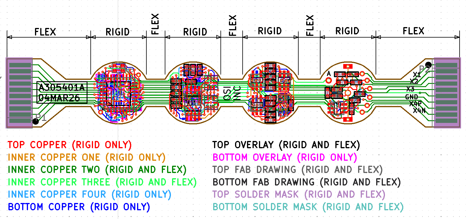
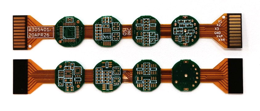
[04-FEB-26] Create web pages. Here is a sketch of the planned three-layer PCB rigid-flex circuit. The board consists of three circular sections joined by two flex cables. The flex cables between the rigid sections are just the right length so that they allow the rigid sections to fold over onto one another without leaving extra flex cable to jut out the side of the implant. On either end there are flex cables with flex connectors at the end. We use the left flex cable to power the circuit and program the logic chip. We use the right flex cable to test the amplifiers.
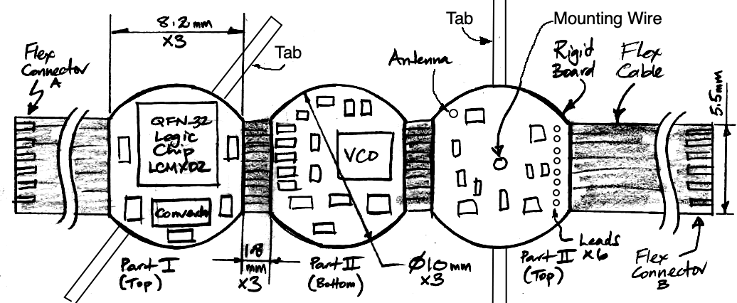
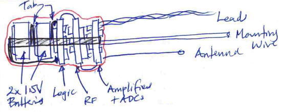
From left to right we have Section I, Section II, and Section III. Each lies within a 10-mm diameter circle and is squared off where the flex cable emerges from its side. The positive and negative battery tabs are on Section I. We tab-weld two 1.5-V SR936 1.5-V 9.5-mm diameter, 3.6-mm thick, 75 mAhr batteries together and to these two tabs to power the circuit, with the positive terminal resting on the logic chip and the negative terminal of the second battery on top. The two batteries are connected by their own tab. We cannot trust to contact to hold them together because the epoxy of encapsulation will penetrate between the two of them. Later, we fold the circuit onto itself, and secure the three layers together by tab-welding the two longer tabs on Section III to the negative terminal of the top battery.
Section I holds the magnetic sensor and transistor that put the circuit to sleep, the logic chip, a buck converter to generate the 1V2 logic power supply voltage, a linear regulator that produces 1.8 V, BMA423 accelerometer, TMP117 temperature sensor, and a converter that provides a battery voltage measurement.
We have a long discussion with ChatGPT about the possibility of using other logic chips, or ready-made micropower MCUs in place of our OSR8 in LCMXO2 FPGA. We consider using in place of the OSR8 the open-source PicoRV32 VHDL processor. This thirty-two bit alternative to our eight-bit processor takes up two thousand LUTs in its usual form, but can be stripped down to 750 LUTs, although in this state it has no memory interface. We consider how long the PicoRV32 will take to perform typical IPT tasks, such as add and accumulate samples, respond to interrupt, and generate random number. We estimate the PicoRV32 will take at least twice as long to perform these tasks, doubling our dynamic current consumption. An advantage of the PicoRV32 is the C-compiler toolchain we can use with it, but we enjoy writing OSR8 assembler, so we have no problem living without a compiler. Another big issue for the implant is the calibrated ring oscillator that turns on and off instantly. These are not available in any existing MCUs, which use RC oscillators, and none of the RC oscillators in the PIC chips we looked at will run at 5 MHz, only 4 or 8 MHz on either side. Our conclusion was that our existing LCMXO2, ring oscillator, and OSR8 is already the most energy-efficient design.
We would like to have spare logic on our device, but at the same time we want to get moving with a flex circuit that does not require microvias to transport IO signals out of a dense BGA. We decide to start our development of the IPT with the LCMXO2-1200ZE in QFN-32, which provides 21 IO pins, enough for the design we have in mind, and is easy to load by hand and work with. Despite the use of this larger package, we expect to be able to load a 1.2-V buck converter using made out of the ST1PS02D, its inductor and decoupling capacitor, on one side of the board, along with a 1.8-V linear regulator. The 1V8 will be used to power the accelerometer and temperature sensor, as well as the logic interfaces of our analog to digital converters, and our antenna switch. The logic chip will have all its I/O pins running off 1.8 V. This is adequate to control our five-bit tuning DAC, the VCO control input, the PE4259 RF switch, and the logic interfaces on our ADS7052 converters.
Section II will hold all RF circuits, while passing through logic signals and power for Section III. We will place near the VCO the five-bit resistor DAC required to provide the VCO's tuning voltage. Also on Section II will be the antenna switch and the crystal radio that produces the received power signal RP. The antenna matching network will be placed between the VCO and the switch, and the switch directly on the antenna.
Section III will hold four amplifiers, each consisting of a single micropower op-amp such as the MAX4464 a few passives, and a ADS7052 converter. Three of the amplifiers, those intended for iEEG, will in addition be equipped with an AC/DC selectors switch DG2012E. Through-hole pads will accommodate up to six biopotential leads, an antenna, and a mounting wire we will use during encapsulation. We would also like to include on this board 2.0-V and 1.0-V linear regulators to provide the amplifiers and converters with clean analog power. By this means, we hope to eliminate the noise caused by the irregularity of our telemetry system's transmission scatter. The dedicated converters eliminate noise generated by selecting one of four analog voltages with an analog switch. A last function we wish to apply to Section III is an electrode impedance measurement with an analog switch that applies a −10 mV step to the iEEG reference potential.
The total surface area of these three boards, counting both sides, is roughly 220 mm2, compared to 150 mm2 for our rounded-corner 12.5-mm square A3049 printed circuit board, which houses two amplifiers with dual op-amps and 3-pole low-pass filters. Our hope is that with the increased area and reduced complexity of the amplifiers, we will be able to fit all IPT circuits on the three-part circuit board.
[06-FEB-26] Working on the A305401A layout. We can fit all the planned components on Section I with 10-mm diameter. We have yet to draw a circuit diagram or route connections.
[10-FEB-26] We have the P3054 repository set up on GitHub. We first worked on the P3041 firmware, fixing instability in its interrupt manager, making changes, recompiling and checking for stability. We create OSR8V4 and perform some consolidation of logic and renaming which, in the end, makes not difference to the compiled code. We start P3054 with P3042 V3.1. The code takes up 1267 LUTs. We reduce the millisecond interrupt timers from sixteen bits to eight bits. Now 1195 LUTs. Eliminate the clock calibrator, which includes an eight-bit counter that counts TCK periods. Our plan is to measure the TCK frequency by watching the state of RCK through the top bit of the status register, thus moving the counter into software. The code remains 1195 LUTs, despite the removal.
[11-FEB-26] We cannot fit all the components we need onto three sections 10-mm diameter along with the antenna mounting hole, lead mounting holes, and tab pads on Section III. We resolve to add Section IV. On this fourth section we place some 0.5-mm tall resistors and one analog switch. These will all be on the top-side of the PCB, which will be folded so that it becomes the end wall of the assembly. There will be no parts on the other side of this section. Now that we have more space, we will make the rigid sections 0.6-mm thick rather than 0.8-mm thick. The flex sections will be 0.1-mm thick.
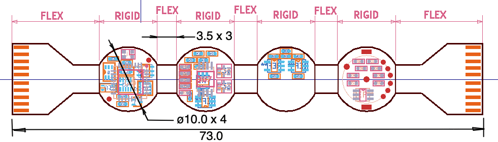
The flex circuits at the either end are 11-mm side, terminated with a ten-way 1-mm pitch single-sided flex plug. The plug on the left carries the seven signals required to program the logic chip, plus three test point signals. The plug on the right carries all the analog signals, of which there are six, as well as the analog power supplies and the Receive Power (RP) signal. The antenna signal enters on Section IV, passes along the flex connector to Section III, passes through Section III, and so to Section II where it is delivered to the RF switch. The length of these tracks will constitute our antenna before encapsulation. After encapsulation, we have this path folded twice, and then a bent cable antenna outside.
Section I still holds the logic, buck converter, accelerometer, temperature sensor, and oscillator. Section II holds the tuning DAC, VCO, crystal radio, antenna switch, and also the four ADCs for the biopotentials. Section III holds the amplifiers and their AC/DC switches. Section IV has pads for mounting holes, and also the resistors that immediately greet the incoming iEEG signals, as well as the impedance-measurement switch and its pair of resistors. We have ample space for soldering leads into six through-hole pads, antenna into its own pad, and the mounting wire. After soldering these wires into Section IV, we trim the understide. We must avoid contact between these components and the parts on Section II. Because Section II will provide epoxy-encapsulated components 1 mm tall, the two boards will be 1 mm apart. The resistors on Section III will be 0.5-mm tall. So we must trim the back side of Section IV so that nothing sticks out by more than 0.4 mm, in order to avoid contact and allow epoxy to provide insulation between the sections. If we load the eight wires with Section IV pressed flat on a flat surface, we should be able to solder them from the top side and avoid any wire protrusion on the other side. All the mounting holes are large enough to allow solder to flow around the leads, antenna, and mounting wire.
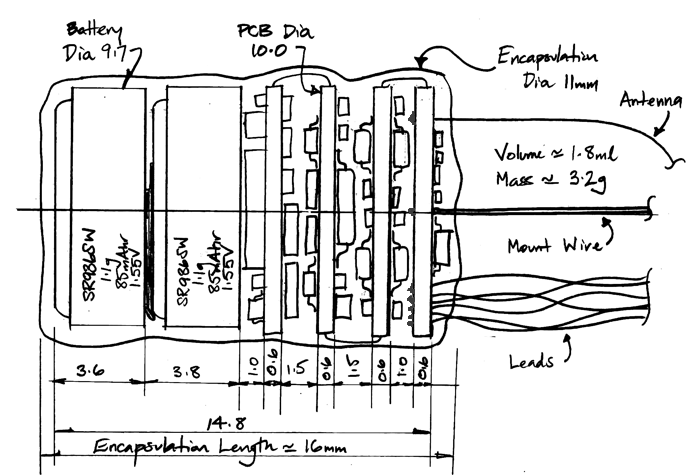
Adding 0.6 mm of epoxy and silicone to the outside of the assembly, all allowing for some indentation between the circuit boards, we estimate total volume will be around 1.8 ml. We calculate the mass by adding the mass of the two batteries to the mass of the rest of the circuit, using for the rest of the circuit a density of 1.2 g/ml. We arrive at 3.2 g total mass. Battery capacity is 85 mAhr = 3500 μA·d at 3.1 V.
We add a 2K×8 EEPROM to Section I, an M24C16-F from ST Microelectronics to act as our non-volatile memory (NVM). We connect this device to the same I2C bus we are using with the BMA423 accelerometer and TMP117 temperature sensor. All three devices are powered by 1V8 and share the same SDA and SCL. We now have two locations for non-volatile storate. The TMP117 contains 48 bits of general-purpose non-volatilve memory (NVM). We can use sixteen bits for the device ID, four bits for a ring oscillator calibration, four bits for an RF center frequency calibration, and eight bits for a battery capacity counter. We still have sixteen bits left for power-up configuration. We will use the M24C16's 2 KByte of NVM to store the IPT's telemetry protocol. This program is written in OSR8 assembler and manages the IPT's behavior when the IPT is active. Upon waking, or in response to a command, the IPT will copy the NVM into its own program memory. When we activate the IPT, it executes the activity program either 1024 times per second, depending upon the IPT's configuration. The activity program reads sensors, accumulates samples, and manages transmission of telemetry messages, including introducing temporal scattering. We note that executing 1024 times per second is about as often as we can hope to do so with the OSR8 running at 32.768 kHz. When the interrupt occurs, the OSR8 will complete its current operation (1), jump to the interrupt location (2), jump to the interrupt routine (3), push accumulator (1), load 0x01 (2), enable TCK (3), boost (3). So that's 15 clock cycles just to start the interrupt in boost. We need another 9 to return from the interrupt. So just servicing the interrupt without any content costs us 24 clock cycles, and we have only 32 between interrupts. Assuming our activity program completes in under 300 clock cycles, it will take 2 clock cycles, leaving 6 clock cycles for the main loop to use to service incoming commands. Somewhere in here we have to fit sample transmission and scatter.
[12-FEB-26] From our OSR8 study of static current consumption, we expect the static current drawn by one of the LCMXO2-ZE devices from our 3.0-V battery at 37°C to be 39% of the typical value presented in Table 3.9 of the MachXO2 data sheet.
| Device | LUTs | RAM KBits | I_q (μA) Tabulated | I_q (μA) Implantable | Packages (Name, mm × mm) |
|---|---|---|---|---|---|
| LCMXO2-256ZE | 256 | 0 | 18 | 7.0 | QFN-32 5x5, ucBGA-64 4x4 |
| LCMXO2-640ZE | 640 | 18 | 28 | 11 | QFN-48 7x7 |
| LCMXO2-1200ZE | 1280 | 64 | 56 | 22 | WLCSP-25 2.5x2.5, WLCSP-36, 2.5x2.5, QFN-32 5x5 |
| LCMXO2-2000ZE | 2112 | 74 | 80 | 29 | WLCSP-49 3.2x3.2 |
| LCMXO2-4000ZE | 4320 | 93 | 124 | 48 | WLCSP-81 3.8x3.8, QFN-84 7x7 |
| LCMXO2-7000ZE | 6864 | 240 | 189 | 74 | NONE |
If we cannot fit our code into the 1200ZE, we will have the option of loading the 2000ZE in its place, and suffer an increase of 9 μA in our static quiescent current. For implants where we do not need the sophistication of the OSR8, such as an upgrade to our existing A3047, A3048, or A3049 SCTs, we could try the 256ZE with only 7 μA quiescent drawn from 3.0 V. Right now, the current consumption of the A3048 is 18 μA + 0.12 μA/SPS, of which 0.07 μA/SPS is the VCO during transmission, 0.01 μA/SPS is the DAC, 0.04 μA/SPS is the logic. The ADC contribution is negligible. If we add the quiescent current of the magnetic switch, op-amps, converter, and regulators, we might get 12 μA from the battery quiescent. Dynamic current consumption from logic will be at most that of an OSR8 plus ring oscillator, which is 1.2 mA * 7 μs = 0.0084 μA/SPS. Combined we get 12 μA + 0.09 μ/SPS. At 256 SPS this implies 35 μA. Operating life with CR1225 rises from the A3048's 41 days to 57 days.
[20-FEB-26] We have completed OSR8 V4.2. We removed eight instructions that we have never used. This size of the CPU by around 60 LUTs. We constrained the logic fully, adding default values for all signals in both combinatorial and synchronous processes. This increased the size of the code by around 100 LUTs. We removed integer types and replaced with unsigned and vector types. We simplified many expressions. We separated the ALU input multiplexer from the CPU into its own process. These changes reduced the size by around 40 LUTs. In the P3041 code, we fixed our asynchronous resets in the interrupt controller. We enhanced the boost controller so that it can start TCK and move immediately into boost. We added to the OSR8 an interrupt servicing output, which we now use to put the CPU immediately and automatically into boost when an interrupt starts, and out of boost when it ends. The P3041 code is now 1201 LUTs. We have 79 LUTs free. The A3054 does not need the A3041's sixteen-bit interrupt counters, nor its millisecond timer. It will not need the TCK calibrator because we have devised a way to calibrate TCK from within software by watching RCK and counting. When we remove these processes, the code shrinks by another 50 LUTs to about 1150 LUTs. We will have around 130 LUTs for A3054 peripheral functions, such as ADC readout.
[23-FEB-26] We are estimating the current consumption of the A3054. Suppose we digitize and accumulate samples from all four fourteen-bit ADCs at 1024 SPS. We now have instant boost and un-boost with FCK running for an average of 4 μs after we un-boost. We can ignore FCK current consumption outside the time required for completion of the interrupt. Using FCK to read out the ADCs, we can obtain a 14-bit sample in no more than 20 FCK cycles, or 2 μs. We estimate no more than 25 TCK clock cycles to read the sample and add to its 18-bit accumulator in RAM. We might be adding up to sixteen samples before transmitting. We use IX and IY to accelerate read and write. We have TCK = 5 MHz so that's 5 μs to read and accumulate. The read initiates the next conversion in the ADC. The ADC itself consumes 0.5 mA at 1 MSPS, so 0.5 μA at 1024 SPS. We have 7 μs of CPU in boost, consuming 1.2 mA from 1V2. With our 80% efficient converter, battery at 3.1 V, and 1V2 = 1.02 V, current from battery is 1.02 V / 3.1 V / 80% = 41% of 1V2 current. So our 1.2 mA is 490 μA from the battery. We need this current for 7 μs per sample per second, so 7 μs * 490 μA * 1/s = 3.4 nA/SPS = 3.5 μA to support 1024 SPS. Each active channel requires 0.5 + 3.5 = 4.0 μA for sampling.
At the end of the sampling interrupt we decide if we are going to transmit one of the channels. If we are going to transmit, we copy the 18-bit accumulator into an 18-bit transmit register and then shift left or right until we get the correct 16-bit sample. This might be the average of sixteen samples or a single 14-bit sample left-shifted twice so it is 16-bit. We set a random delay interrupt of 0-7 RCK cycles to produce transmission scatter. These tasks take another 25 clock cycles, or 5 μs, which is 2.5 nA/SPS transmitted. Our sample interrupt ends and the tranmit interrupt occurs a random time later. Right now, our boost controller does not allow us to leave boost during transmission. The transmission takes 7 μs at 10 mA from the battery directly for the VCO and about 10 μs at 1.2 mA from 1V2 for the CPU in boost. We have 7 μs * 10 mA * 1/s 70 nA/SPS for the VCO from the battery and 10 μs * 1.2 mA * 41% = 5 nA/SPS from the battery for the CPU, for a total of 75 nA/SPS transmitted.
The quiescent current of the LCMXO2-1200ZE at 37°C is 56 μA from 1V2. Add to this another 14 μA for the crystal radio, amlifiers, accelerometer, thermometer, and NVM, we get 70 μA. From the battery this will be 70 μA * 41% = 29 μA, say 30 μA. Combining this with the above 4.5 μA/Ch (per active input channel) and 75 nA/SPS transmitted we have:
I_a = 30 μA + 4.5 μA/Ch + 0.075 μA/SPS
Suppose we have one active channel at 256 SPS, our current is 53 μA, which is a little over the 48 μA maximum of the A3048S2. But here we are going to be adding four 14-bit samples to obtain a very fine 16-bit sample, far superior to the spikey sixteen-bit samples we obtain from the A3048. Now suppose we have two active channels at 512 SPS. Our current is 115 μA, which is less than the 22 + 1024 * 0.11 μA/SPS = 135 μA of the equivalent A3049 two-channel circuit.
[26-FEB-26] Schematic for A3054AV1 drawn. There are twenty-one programmable pins on the LCMXO2-1200ZE in QFN-32 we are deploying on the A3054AV1 as U4. We will use all of them. Four must be shared with the programming signals TMS, TDI, TCK, and TDO. These we assign to the D0-D3 bits of our five-bit tuning DAC, on the grounds that they will be loaded by at most 2 kΩ and driving them during programming will cause no harm. The programming cable will use the JTAG Enable pin, which we call PEN, on U4-26, to switch these outputs from their programmed to their programming functions. We have nineteen pins that are necessary for the functioning of the IPT and we use the two remaining pins for an indicator lamp, signal LED, and at test point, TP. The LED and XEN signals must be 3-V logic, so we assign these to IO Bank 3, which provides exactly two pins, and power VCC3 with VS ≈ 3.0 V, the switched battery voltage. The other three IO banks we power with 1V8 = 1.8 V. The core VCC we provide with 1V2 = 1.20 V on startup and later with the assertion of LV becoming 1.0 V.
[04-MAR-26] Layout of the A305401A complete. We had to use six layers in the rigid sections, but were able to manage with only two in the flex sections. We used one via in the flex sections to complete the layout, having determined from our fab house that vias in the flex sections are standard. The entire rigid-flex circuit is 73 mm from end to end and 11 mm high with its two flex cables. Once the IPT is programmed, calibrated, and configured, we will cut off the flex cables, leaving four 10-mm diameter sections joined by 3.5-mm flex cables.
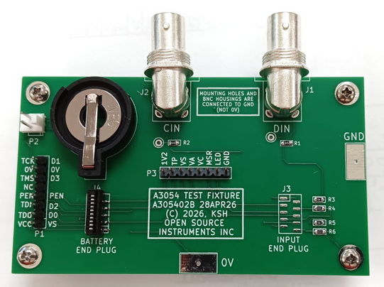
Before we make the rigid-flex A305401A we will make the rigid-only A305402A, which will include the A305401A layout on a 1.6-mm thick rigid board, along with two 10-way flex sockets, an eight-way programming plug, a two-way power plug, a BNC socket to bring in an analog signal for the IPT inputs, and various other pin headers for calibration and testing. This board will serve as a test of the IPT circuit, but in the future serve as our programming and calibration test fixture. Once our A305401A netlist has been double-checked against the schematic we will proceed with the A305402A layout.
[05-MAR-26] We complete the layout of the A305402A test fixture circuit board, which we will use to build the A3054X breadboard version of the IPT and the A3054TF test fixture for programming and quality control. There are many test points on the circuit board. Those marked in the larger font are available in the test fixture version, when we plug a rigid-flex IPT into the flex sockets on the left and right. Those marked in the smaller font will be available when we build the A3054AV1 circuit on the test fixture circuit board for our first tests.
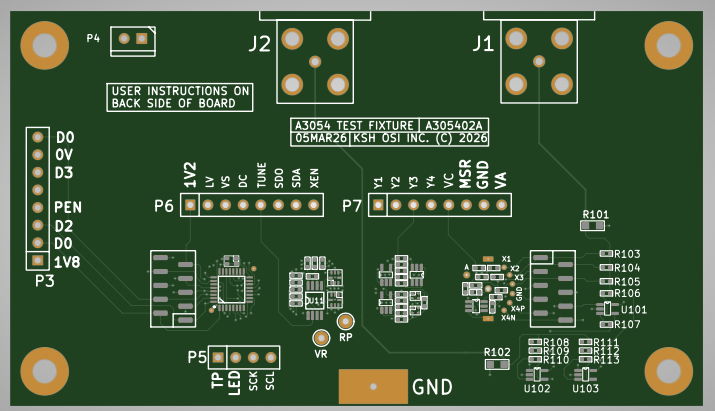
In addition to a programming plug for the logic chip, a power plug for bench-top or battery power, and numerous test points, the test fixture provides two BNC sockets for delivering a differential signal and a common-mode signal to the A3054 amplifiers. These are DIN and CIN on the schematic S3054X_1.gif. We terminate DIN with 51 Ω and deliver through 1.0 MΩ to X1, X2, and X3, where the input impedance of 1.0 MΩ will divid the terminated signal by two. We take DIN and invert it with respect to VC. We assume that we will be delivering DIN, the differential input, with an offset of VC = 0.90 V, which we can do easily with our analog signal generator. We now have DINM and DIN, a differential signal about VC. We shift both of them downwards by CIN-VC and connect them to X4P and X4N. Now we can apply a true differntial signl to X4P and X4N as well as a true common mode signal, all without unplugging anything or reconnecting anything, under the control of our analog signal generator.
[16-MAR-26] We are waiting for the A305402 and going about securing all the parts we need to build the prototype on the test board. While welding batteries onto SCTs today, we started to re-think our plan to have the IPT hibernate on a magnet, but always be running when it is not attached to a magnet. After welding the battery taps on the IPT, we will encapsulate in epoxy, touch up epoxy, and coat twice with silicone. This process takes at least two days, and sometimes four days. During that time, the IPT will be awake and consuming 15 μA. We might lose up to 1.4 mAhr of battery life during encapsulation. Now, when we want to soak them in water to check the coating, we can leave them for another one to three days soaking while awake, or we might make a container with individual magnets in the bottom to hold the IPTs while we cover them with water to soak. There may be several more problems with our hibernation plan that we are as yet unaware of. The ISTs in which we first implemented the hibernation model had waking current of only 5 μA, so we concluded the loss during encapulation was tolerable. We may be better off adding a flip-flop to the sensor output so we can drive the mosfet switch on and off as we bring the magnet near.
[24-MAR-26] We receiver our A305402A boards. We load U1 and Q1 and 10 μF capacitors using paste and oven. Our SOT-723 footprint, which we copied from KiCad libraries, has a pin assignment that does not agree with our tradition, and as a result the transistor is connected incorrectly.
[25-MAR-26] Short Q1-1 to Q1-2 with a wire link. Load U2, we now have U1 (not used, but working), Q1 shorted, C1 = C3 = 10 μF, C2 = C4 = 1.0 μF, L1 = 2.2 μH. Load 10 kΩ from 1V2 to 0V. Have LV input floating. Connect 3.0 V to VB. Measure 1V2 = 1.01 V, VB current I_VB = 43 μA. Meanwhile, 1V2 current must be I_1V2 = 101 μA. We add 33 kΩ in parallel with our 10 kΩ load, adding 31 μA to I_1V2. We see I_VB increase to 57 μA. Differential conversion efficiency is 31 / (57 - 43) * 1.01 / 3.0 = 73%. Absolute efficiency, including magnetic sensor current, is 132 / 57 * 1.01 / 3.0 = 78%.
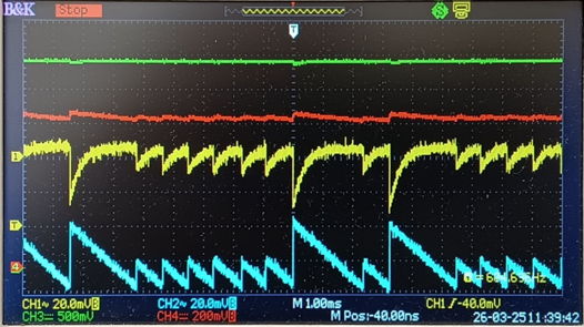
The battery voltage VB = VS on the circuit is stepping down when the converter connects its inductor to VS, while 1V2 steps up. These steps are usually 18 mV but sometimes 36 mV. Following a large step up, we have relaxation at 36 mV / 2.2 ms = 16 V/s as our 101 μA load drains C3, implying C3 is behaving like 101 μA / 20 V/s = 6.3 μF. We examing the AC-coupled VS and 1V2 as well as the switching side of the inductor. A 36-mV step up is one where the converter applies two pulses to its inductor rather than just one. This happens roughly 10% of the time. Otherwise, the converter, U2, applies one pulse and generates an 18-mV step up. When VS steps down 36 mV, 1V2 steps up 36 mV, which suggests the charge is being transferred from C1 = 10 μF to C3 = 10 μF with no loss.
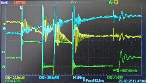
When U2 connects L1 to VS, we see VS dropping as C1 discharges while 1V2 rises as C3 charges up. When the converter connects L1 to 0V, L1 continues to pump current into C3. After the second pulse on L1, we have U2-3 connected to 0V for 500 ns as it discharges its energy into C3. When U2 releases L1, the inductor still has some energy left, and drives its current through a Schottky diode in U2. When it is exhausted, L1 causes U2-3 to ring for a few cycles before settling to 1V2.
We load U3 and C4 and get 1V8. We load U4 and U4. We set up P3054 firmware, starting with the latest P3041. We remove stimulus code from ROM.asm and add a pulse on df_reg(1) to mark the main loop. We program U4. We see 1V2 = 1.20 V and I_VB = 38 μA with LV driven LO. Reprogram and drive LV HI. We now have 1V2 = 1.02 V and I_VB = 22 μA at 25°C. We see our pulse on TP showing the main loop execution. We warm to body temperature, I_VB increases to 28 μA.
[31-MAR-26] We abandon our "hibernate on a magnet" plan. We remove the 1V8 power supply, which eliminates a regulator and a capacitor. We use VS in place of 1V8 everywhere. We add a flip-flop in UDFN-6 package. We can now turn the A3054 on and off with a magnet, and we still have a mosfet switch. We move the oscillator to the bottom side of the IPT layout so it won't tilt the battery.
Meanwhile, we press on with the A3054X breadboard. We set frequency_low to 24 in ROM.asm. We try the auto-calibration of TCK and get TCK period varying from 163-184 ns with the ripple in 1V2. The entire message transmission is 6.06-6.82 μs. We have 50% reception. We replace the old divider-based ring oscillator with the new many-gate ring oscillator we developed for 1V2 = 1.0 V in the P3051 firmware. We delete the Clock Calibrator process from Main.vhd. Our compiled code is 1168 LUTs. We set fck_divisor = 24 and period of TCK is 197-227 ns. If we decrement or increment fck_divisor, the period is too short or too long. The variation is due to ±18 mV ripple in 1V2.
[01-APR-26] Our A3054X is using its multiplier to transmit the square of sample number, which we see on the Receiver Instrument. Our TCK is 212±15 ns, or ±7%. We have 36 mVppo ripple in 1V2. In place of P0603 2.2 μH for L1, we load P0805 4.7 μH. We now have TCK 216±10 ns with 20 mVpp ripple. Increase C4 to 20 μF, TCK is 218±4 ns, which is ±2%. Ripple in 1V2 is down to 10 mVpp. We drop transmit rate to around 105 SPS. Quiescent current is 33 μA with our 4.7 μH and 20 μF. With 4.7 μH and 10 μF, 35 μA. With 2.2 μH and 10 μF, 36 μA. With 2.2 μH and 20 μF, 35 μA, TCK is 217±6 ns, 1V2 ripple 16 mVpp. Go back to our P0805 4.7 μH and load 22 μF for both C1 and C3. Current is 32 μA, TCK is 223±5 ns, or ±2%. We examine the 1V2 ripple with a ×1 probe, 2.7 mV rms, 13 mVpp, but at the time of transmission, the value varies by 10 mVpp. We drop fck_divisor from 24 to 23 and now have TCK 194±4 ns. The drop in TCK period from fck_divisor 24 down to 23 is 13% when the decrease in the number of gates in the ring oscillator is only 4%.
Our A3054X is consuming 32 μA while transmitting 110 SPS and calculating a square for each sample. We remove the multiplication and instead just increment a register and transmit in place of both low and high bytes of the sample. With the removal of the multiplications, current consumption drops from 32 μA to 28 μA while sample rate remains 110 SPS. Each multiplication costs 36 nC from the battery. We increase sample rate to 185 SPS and current increases from 28 μA to 35 μA. The transmission cost is 0.093 μA/SPS. Extrapolating back to 0 SPS, the static current consumption at 25°C is 18 μA. P3054 commit 0b346e2.
Add crystal radio and comparator. Remove regular sample transmission. Current 22 μA at 0 SPS. The A3054X responds to a request for identification, but does not at first turn on its transmitter. We start again with ROM.asm copied from P3041. We disable the clock calibration. We change frequency_low to our value 24. We set the ID to 0xAA55 for its distinctive bit pattern. We restore the Stimulus Controller to Main.vhd and replace On Lamp (ONL) with LED. We put a dummy response in place for a battery measurement to give an apparent 3.0 V. We load a white LED for D3. Test all functions, everything working: transmit, stimulus, acknowledgements. We measure battery current versus sample rate and get a slope of 84 nA/SPS.
[02-APR-26] Load U7 TMP117, the temperature sensor. Add I2C code to ROM.asm, copying from P3051. Our program is now 2900 bytes. The total program memory is 4096 bytes. In the A3041, we use the bottom 2048 bytes for the main program and set aside the top 2048 bytes for the user program. We write a "ret" instruction to location 2048. We can no longer tolerate this "ret", so we comment it out. We are configuring and reading the temperature sensor. Firmware v1.3.
Our I2C interface is running at 5 MHz / 9 = 555 kHz when the maximum specified for the TPM117 is 400 kHz. But the sensor measurements are being read out correctly: we see 24.9°C. Here is an example of one of our SCL pulses on a single-bit read. Each instruction has the numer of CPU clock cycles next to it, and the CPU is running at 5 MHz.
ld (mmu_i2cZ0),A  ; 3
ld (mmu_i2cZ1),A  ; 3
ld (mmu_i2cZ0),A  ; 3
The total time for the read is 490 clock periods including the call and return, or 98 μs. The ring oscillator and CPU together consume 1200 μA from 1V2, or 1200 μA * 1.02 V / 3.0 V / 80% = 510 μA from VB = 3.0 V. Each TMP117 readout requires 98 μs * 510 μA = 50 nC of charge. The readout cost of sampling is 50 nA/SPS. Add the transmit-only cost of 84 nA/SPS and we get 134 nA/SPS. Our actual cost is 140 nA/SPS, so we assume the extra 6 nA/SPS is consumed by the I2C interface and the TMP117 itself.
[03-APR-26] We use the TMP117 temperature sensor loaded on our A3054X to measure static current consumption versus temperature. We start by putting the A3054X in our oven, removing, connecting it to power and wrapping in insulation. We watch current consumption from the battery at 0 SPS then turn on transmission of the temperature measurement. To get the colder temperatures, we place two ice packs on either side of the A3054X and wrap with insulation.
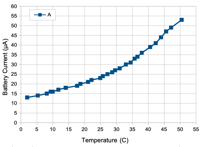
The quiescent current at 0 SPS is the "wake current" of the IPT, in which it is awaiting commands but otherwise doing nothing. The wake current is around 34 μA at 37°C. We configure the TMP117 to provide a new measurement every 15.5 ms, which is its specified typical conversion time, and now we see noise on the temperature measurement we receive at 256 SPS. Current consumpton is around 220 μA, suggesting the TMP117 consumes 160 μA when producing 1 / 15.5 ms = 64 SPS. The TMP117 data sheet says current consumption during active conversion is typically 135 μA and the sensor is converting as fast as it can.
We load U6, the BMA423 accelerometer. We spend the day trying to get it to respond to our I2C bus. For a few seconds it responds at one point, then stops. We conclude that the device is not configuring for I2C because we failed to tie U6-10 CSB to VDD. The data sheet says that we can leave this pin "VDDIO or NC (float)" to get I2C instead of the SPI interface, but recommends we connect it to VDDIO. In their application circuits, CSB is connected to VDDIO for I2C. So we solder 125-μm bare silver wires to one of the devices and make three connections to 0V, three connections to VS, and connect SCL and SDA as well.
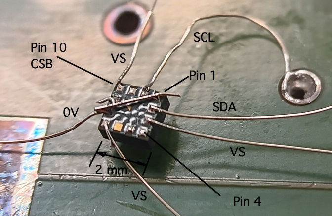
We still fail to communicate correctly. The device does not respond nor acknowledge our I2C cycles when we have probes on SDA and SCL. We are trying to read register 0x00, the chip_id = 0x13. We are transmitting 32767, which means we are reading 0xFFFF from SDA. In our software, we add 0x1000 to the value we read from the accelerometer so as to offset the accelerometers two's compliment range −32768..+32767 to our unsigned sixteen-bit range 0-65535. When we remove our probe from SCL, however, something starts driving SDA. We see the bits in our trace of SDA alone. We are transmitting a value 37632. We are reading 0x13 from register 0x00 into our top byte and a reserved byte from register 0x01 into our bottom byte. Assuming the reserved byte is zero, we expect to get (19 * 256) + 32768 = 37632. So it appears we are communicating with the BMA423 now that we have CSB = VS. We remove the wired chip, clean, dry, and return to our TMP117 either shut down or converting at 64 SPS with 256 SPS transmitted. When shut down, current is 23 μA. In the S3054_1 schematic, we connect U6-10 (CSB), U6-4 (ASDA), and U6-11 (ASCL) to VS. The latter two we connect so we can get to U6-10, and the data sheet says we can connect these to VDD if we are not using the secondary interface.
[07-APR-26] Load U8, M24C16, our 2K × 8 EEPROM. Its I2C device address is 0x50 for the first 256 bytes and 0x57 for the eigth. We are able to write 0xA5 = 165 to byte zero on start-up and then read it back again repeatedly for transmission. The second byte we read is 0xFF, which is consistent with erasing a sixteen-bit page and writing the first byte with 0xA5. The next fifteen bytes will be 0xFF. We are transmitting 0xA5FF = 42495, which is what we see in our Receiver Instrument.
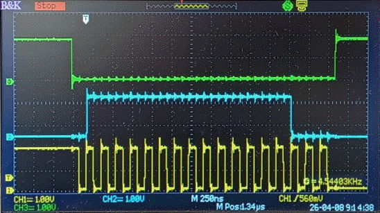
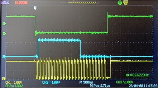
[08-APR-26] We load U12, ADS7052, the first of four 14-bit micropower converters. We connect VA to VS because we don't have the VA regulator loaded. We have nothing connected to the ADC input. We read the ADC and transmit. We see value 16383 = 0x3FFF. We connect the ADC input to 0V with a 10-MΩ probe and the value drops to zero. The ADC readout is shown below for 0x3FFF. The readout is driven by FCK at 10 MHz. We have SCK and !ADC1 HI during idle. At the start of the readout, !ADC1 goes LO. After 100 ns, SCK goes LO as well, and SCK proceeds to run at 5 MHz for 17 rising edges, then goes LO. We see the ADC producing a 0 on SDO until the first rising edge on SCK, fourteen 1s on the first fourteen rising edges, and three zeros on the final three rising edges. Now SCK remains LO and !ADC1 goes HI. Not seen in the picture is SCK going HI again some a little later. The entire readout takes 3.3 μs.
At power-up, we will get all four ADCs to self-calibrate by performing a readout of twenty-four bits, which requires twenty-three rising edges on SCK before we unassert ADC1. The picture below shows a calibration cycle. We see nine zeros being clocked from the ADC at the end of the cycle. At startup, we sould see all zeros from the ADC, but this is not a startup calibration, it's a calibration cycle performed after we have sampled from the ADC. This calibration cycle as shown will not, in fact, provoke a self-calibration. Only the first access after power-up can we used for self-calibration with twenty-four bit readout. If we want to self-calibrate again, we must read out sixty-four bits. Our firmware does not support re-calibration at the moment, only calibration at start-up. At the end of the cycle we see !ADC1 going HI and SCK going HI after another 200 ns.
When we read the ADC, the data is available in 3.3 μs. But the ADC readout state machine, as it exists now, will not be available to read another ADC until a total of 4.5 μs after the start of the access. Given that our CPU must fetch and store the sample, this extra 1.2 μs, which is 6 CPU clock cycles at TCK = 5 MHz, will not slow us down.
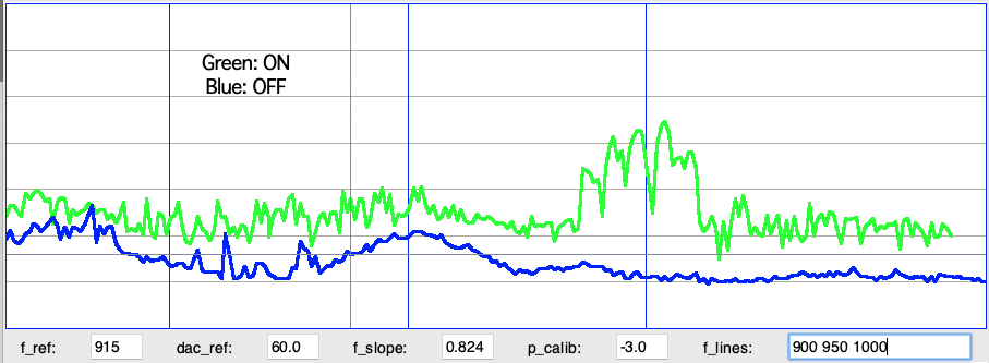
Load remaining three ADCs, the VA and VC regulators, amplifiers and analog switches. We control the ADCs with an eight-bit register in which we have functions for six of the bits. Bits zero and one specify the ADC. Bit two tells the ADC Controller to begin an SPI bus access. Bit three tells the controller to continue the access for twenty-four bits, but not to store those bits in the ADC data register. With bit three cleared, the controller stores fourteen bits in the data register. With bit four set, the controller shifts the fourteen bits once to the left. With bit five set, the controller shifts the bits left once again. We start with ADC1 and shifting twice to the left. We power with a battery, turn on transmission at 256 SPS. We look at SCK to measure TCK and see 199-207 ns. The peak of our spectrum is 915 MHz. We see 240 SPS received. We have frequency_step = 1, which is suitable for DAC voltage 3.0 V, but we have DAC voltage 1.8 V on the A3054X, so we set frequency_step = 2. Reception rises to 252 SPS. On the transmitted signal we see average value 33023 cnt with noise 7.5 cnt rms.
We note that MSR and DC are not being set by our code, so we drive them LO, selecting AC coupling and GND connected to VC. We reprogram. With bench power 3.0 V quiescent current is 29 μA at 25°C. In our Faraday cage, running off a battery, we see 252 SPS and 7.5 cnt rms noise. The gain of our amplifier is ×62. Our VA = 1.82 V. Our input dynamic range is 30 mV. This 7.5 cnt is 3.4 μV rms. In the Neuroplayer, we filter 1-80 Hz and see 2.5 μV noise. In the noise we see traces of quantization, but no spikes. The spectrum is flat. In the noise sample below, we receive 251 samples, so fill in 5 to make 256. But there are more than five places where the signal stays at the same value from one sample to the next. These flat segments are quantization artifact.
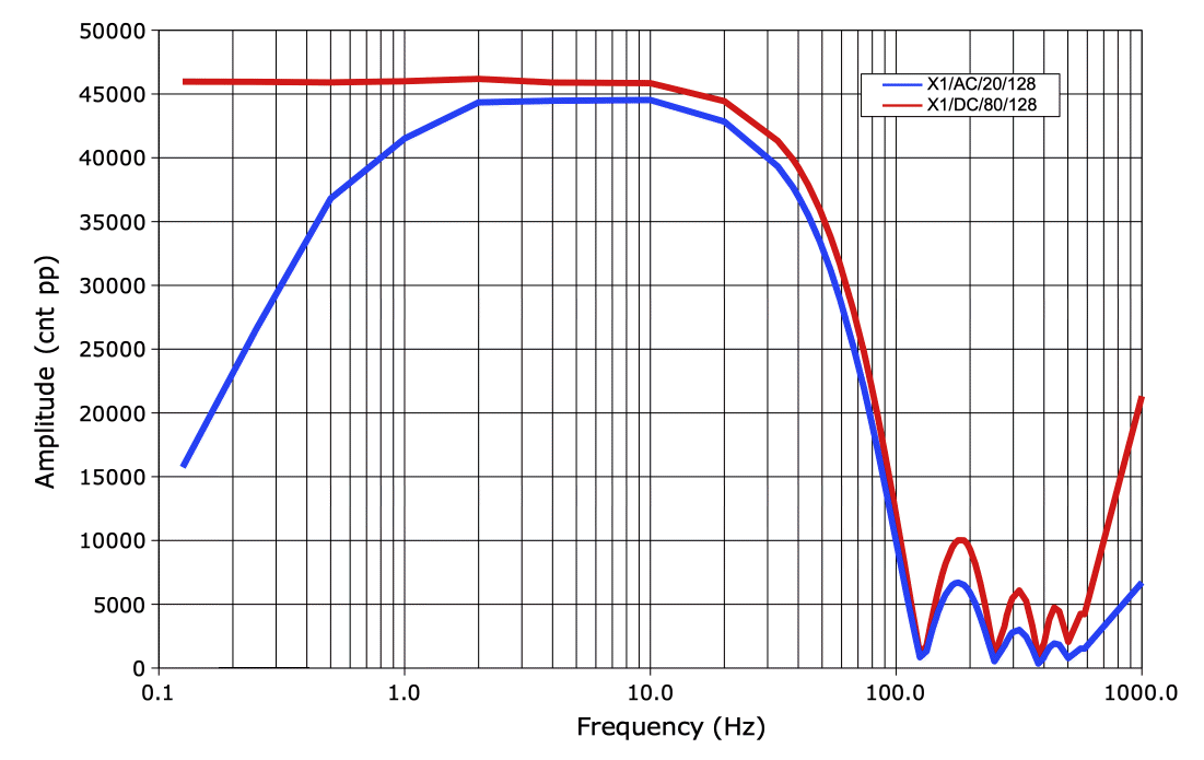
We load external amplifiers that drive the X1-X4 inputs and load two BNC sockets. The amplifiers contain 100-kΩ resistors and with nothing connected to J1 or J2, we have 0V driving their inputs, which leads to current through the resistors, adding about 70 μA to quiescent current consumption of the board. We look at a frequency sweep. The gain at low frequencies is lower than we expect. We see relaxation in response to a 1-Hz square wave with time constant around 100 ms. We remove C14 and C15. We program with DC asserted. We should now have gain ×16 down to 0.0 Hz. We apply a square wave. We see the intact square on U18-1 and U18-3, but on Y1 we see relaxation with time constant around 300 ms. The DC gain is not zero, but is around ×5, while the gain at 10 Hz is around ×16. We perform a sinusoidal sweep, applying a 91-mVpp sine wave to X1 by delivering 100 mVpp with 1.8-V offset to the A3054X's DIN input. We leave CIN open circuit. In the center of the passband we see amplitude 55 kcnt, which is 1.5 Vpp at the amplifier output, or 94 mVpp at the amplifier input. The gain in the middle of the pass band is correct. It is the low-frequency gain that is wrong.
Amplitude We connect U21-6 directly to VC with a wire. We still see relaxation in square wave response. We repeat our sweep and obtain an identical response. We see VC moving up and down. The VC regulator can supply current, but it cannot sink current. Our external circuits on S3054X_4 do not draw current from VC = 0.9 V. Our amplifiers on S3054X_3 draw current when our X1-X3 and X4P inputs deviate from VC. When these are VC + 50 mV and DC is asserted, the total current flowing into VC will be 3 × (50 mV / 133 kΩ) for X1-X3 and 50 mV / 2.1 MΩ for X4P, making 1.1 μA in all. This will charge up C11, which has a nominal value of 22 μF but when we measure the capacitors, we get 13 μF. The charge rate will be 1.1 μA / 13 μF = 88 mV/s. Time constant is around 560 ms, expected corner frequency 0.28 Hz, which is pretty much exactly what we see in the plot above. One solution to this problem is to place a resistor from VC to 0V that draws enough current to supply the amplifier feedback networks. So long as the main feedback resistor is 2.0 MΩ, the feedback current can be as high as 0.9 V / 2.0 MΩ = 0.45 μA, so total could be 1.4 μA. This would add to our quiescent current. Another is to replace U17 with a resistor divider buffered by an op-amp. We might need a capacitor on the divider as well. We can fit the resistor on easily, there is space on section S4. The divider solution may not fit.
We note another problem with our A3054 design, in which we eliminate 1V8 and replace with VS. If we were to make this replacmenet, we would drive DC and MSR with VS = 3.0 V when the analog switches are powered by VA = 1.8 V. One way to solve this problem is to use VS to power the switches. We already have VS on section S3, and it will be no problem to bring VS to S4. We modify S3054A_3 to apply VS to all four switches and make the changes to the A305401A layout.
[09-APR-26] Connect 33 kΩ from VC to 0V. Relaxation of our square wave response disappears. We now get stable response down to 0.0 Hz. We repeat our sweep and call it "DC/91mV/0pF" to indicate DC input, 91-mV on X1, and C15 = 0 pF. We are using 100 mVpp sine wave with offset 1.75 V applied to J1 on A3054X, J2 open circuit. The 100 mVpp passes through 100 kΩ to the 1 MΩ input resistor of the X1 amplifier, and so drops to 91 mVpp. We load C15 = 220 pF and repeat the sweep. The amplitude is slightly lower in the pass-band. Load C15 = 100 pF and repeat. Switch to AC and apply 30 mVpp to J1 with the same 1.75 V offset.
The low-pass corner frequency for our amplifier with AC-coupling and no filter capacitor is about 160 Hz. We would like to provide up to 160 Hz for AC coupling, so we must eliminate the capacitor. With DC-coupling and no capacitor, the corner frequency is around 640 Hz. If we want to deliver 160 Hz with DC coupling we must take the average of four samples. The corner frequency we are seeing is due to the gain-bandwidth product of the OPA369, which is 12 kHz. We expect to see AC corner frequency 12 kHz / 62 = 190 Hz and DC corner frequency of 750 Hz. So long as we stick with the OPA369, we can allow the op-amp to perform our filtering for us. We can eliminate C15, C17, and C19.
We change resistors on external amplifiers for 1 MΩ, including those in series with our X1-X3. We remove R102 and let the common-mode voltage float at 0.9 V. Quiescent current is 33 μA at 25°C. We have 500 kΩ from VC to 0V across C11, consuming 1.8 μA. The external op-amps and resistors consume about 2.7 μA. The remaining 29.5 μA. We reprogram the board so that it transmits X1-X4 with AC coupling for channel numbers 1-4, and with DC coupling for channel numbers 5-8. With channel 9 we read the temperature sensor.
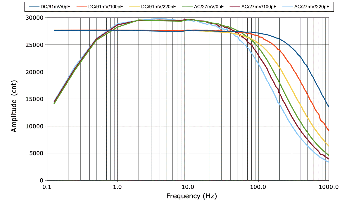
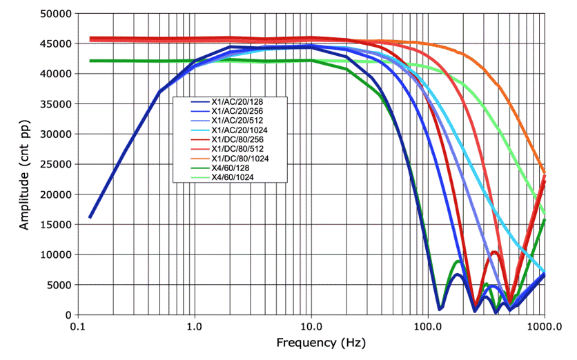
We sweep all the amplifiers to see their frequency response without any feedback capacitors. At this point, we change the vertical axis of our sweep plot to amplitude peak-to-peak. The X4 channel is DC-coupled. Our external circuits generate a differential signal with common mode voltage VC. The differential gain of the X4 amplifier is ×20. The input dynamic range is 1.8 V / 20 = 90 mV. For our 80-mV input we see output 60 kcnt peak-to-peak and we expect 65535 * 80 / 90 = 58 kcnt.
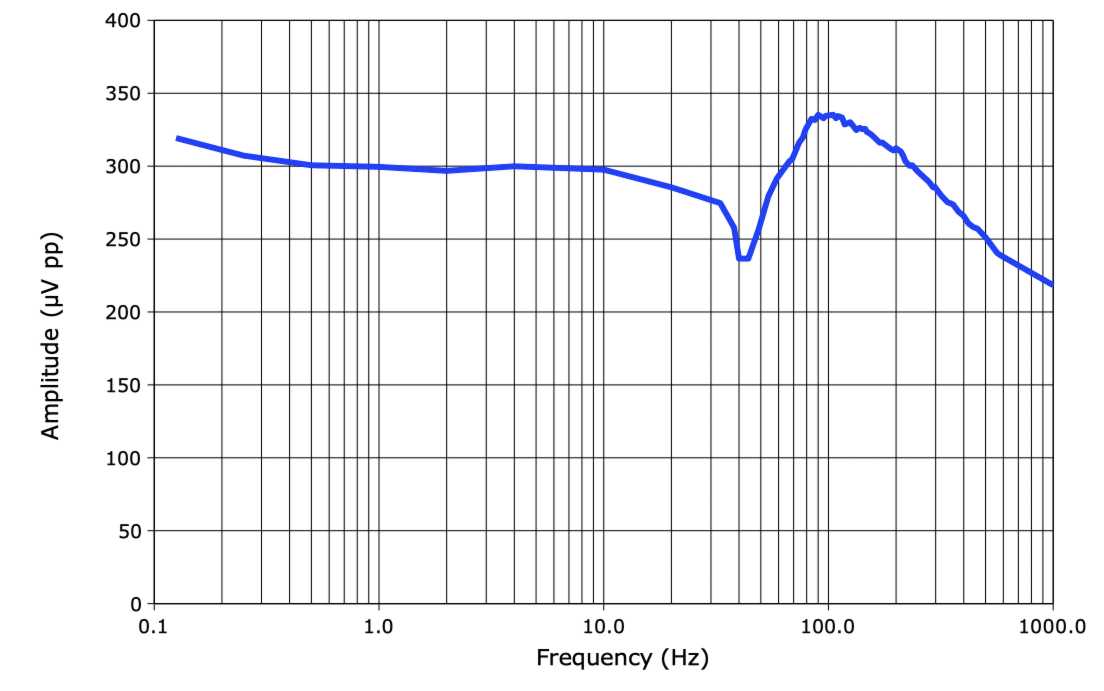
We have no low-pass filter capacitors on our op-amp feedback resistors. All low-pass corners are due to the OP369 itself, and are a frequencies inversely proportional to gain. We have adjusted the input amplitudes so that the amplifier output in the center of the pass band is close to 60 kcnt peak-to-peak for all of channels and configurations. The half-power frequency, which is a traditional measure of corner frequency for low-pass filters that roll off gradually, is the frequency at which the amplitude drops to roughly 42 kcnt pp. The AC-coupled X1-X3 have their corner at 160 Hz, the DC-coupled X1-X3 at 640 Hz, and the DC-coupled differential X4 at 500 Hz.
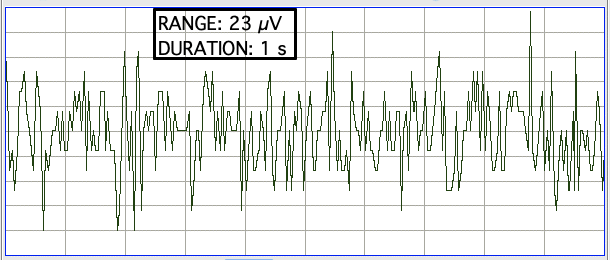
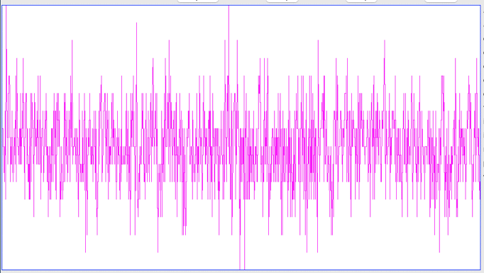
We remove R101. We have already removed R102. The fact that we are grounding our incoming test signals to 0V, but our amplifier ground is 0.9 V, has proved difficult. We now want to measure noise in isolation, so we disconnect these resistors and allow the inputs to be driven by our floating resistors. Input noise at 1024 SPS is 11 cnt rms = 5 μV rms in AC-coupled X1-X3, 9 cnt rms = 15 μV rms in DC-coupled X1-X3. In the DC-coupled signal's noise we see the quantization lines in an amplified picture. There are no random, large spikes.
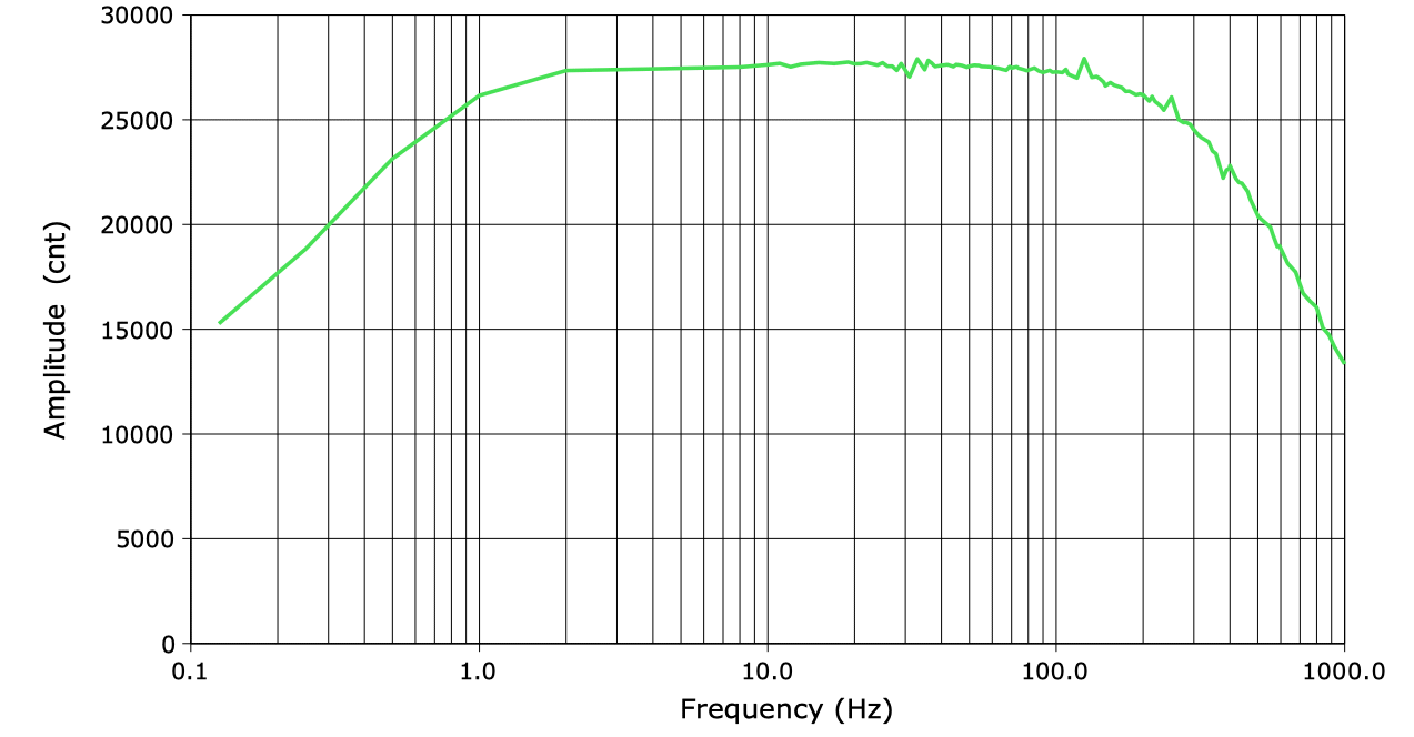
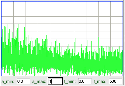
We obtain the spectrum of X1 with AC coupling. With no filter, the noise amplitude is 5.0 μV rms. With low-pass filtering at 640, 320, 160, 80, and 40 Hz, the noise is 4.6, 4.0, 3.2, 2.4, and 1.7 μV rms.
We have on board a white LED in series with 1.0 kΩ that we can drive with our LED logic output. This output takes the place of ONL in our stimulator code, which still exists in P3054 V1.4, even including random stimuli. The lamp power modulator uses RCK to modulate the average light current from 0% to 100% in fifteen steps. We turn the LED on full power and take a look at the AC-coupled X1 signal, which is open-circuit.
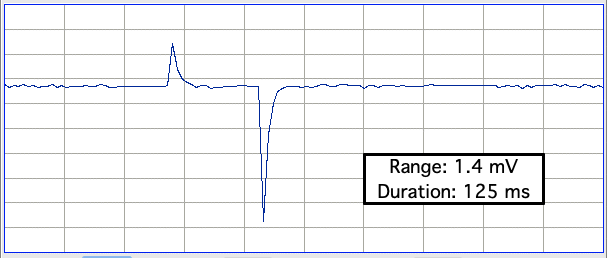
We decrease the power to 50%. Now the lamp current is being modulated during the pulse. This modulation creates an additional new 140-μV pedestal artifact during the pulse.
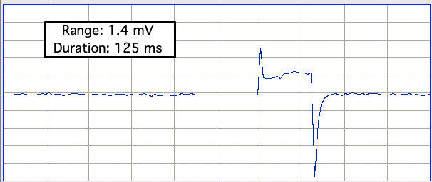
We modify the P3054 software so that the lamp never gets turned on, but instead, whenever the stimulator code would turn on the lamp, it asserts MSR, leaving DC as it is. When we transmit a signal, we leave MSR as it is and construct DC and the input selection from the channel number. We load 16 kΩ for R30. When we assert MSR, GND drops by 7.14 mV. We remove R103, R104, and R105. We connect X1 to GND with 1.0 MΩ, X2 with 2.0 MΩ, and X3 with 16 kΩ. We measure the step down with MSR for AC and DC coupling on all three inputs. We calculate the electrode impedance from the size of the step.
It looks like we can measure the input impedance with a precision of better than ±1% of Z_in, which in our case is 1% of 1 MΩ, or ±10 kΩ. With AC coupling we get 20 kΩ for our 16 kΩ electrode impedance.
We see now that the impedance measurement circuit draws 0.9 V / 2 MΩ = 0.45 μA from 0.9 V. To support the amplifiers, we need to be able to provide a sink for 3 * 0.45 μA for X1-X3 and for X4 we might have X4N = X4P = 1.8 V, which would draw another 0.45 μA. That's almost 2 μA. If we drop R31 to 500 kΩ and R30 to 4 kΩ, we will have the same step size, almost 2 μA available to sink current out of VC, no additional components added to the circuit, and our VC remains stable as the resistors corrode. The additional cost is 1.5 μA over our original design. If we add an op-amp with 4-MΩ divider, we add around 1.2 μA and our VC will drift with corrosion of the divider. Quiescent current of the board at 25°C should be 29 μA.
[13-APR-26] We believe we have settled the A3054 circuit. Layout A305401A is complete. We will await netlist check, then submit for fabrication. We start work on a new text fixture board. We want to eliminate the external op-amps so we don't have to consider their current consumptikon. We will ground the incoming BNC signals to GND and test the amplifiers only when we have the circuit powered by a battery. We terminate the incoming signals with 51 Ω, then divide by 100 with 1 MΩ and 10 kΩ. We have J1 for the X1-X3 and X4P input. We have J2 for the X4N input. By applying opposite signals to X4P and X4N we can apply a purely differential signal to X4. Now we don't need any op-amps to shift or amplify or negate the incoming signals. We will have a 0V pad and a GND pad for scope probes. During MSR, we must be powered by battery. The VC potential will step down by 7.14 mV with respect to GND, as will VB, VS, and 0V.
[21-APR-26] Rigid-flex A305401A under review at fab house. We try inductor MBKK1608T4R7M, 4.7 μH in P0603 package. Prior to replacing the P0805 inductor we had loaded in place of L1, we see sustained and uniform 10-mVpp ripple, in which we have a sharp step up and a gradual decline. Quiescent current is 33 μA. We replace L1 and see ripple that is 12 mVpp but almost all steps are 4 mV with occasional 12 mV steps. Quiescent current is 33 μA. Telemetry reception is 98%, which is as good as it was before replacement.
[29-APR-26] Test fixture schematic S3054Y_1.gif complete. We have removed all the op-amps. The connector chassis and mouting holes are connected to GND. Unless we are measuring electrode impedance, GND will be connected by the A3054 IPT to VC. We have a battery holder on board that will accept a CR2032 battery to power the board. While programming, we will connect an external computer power supply ground to 0V. During programming, we must not connect DIN or CIN to a grounded signal generator. Doing so will short VC to 0V. Once the device is calibrated, we disconnect the programming connector and connect signals to DIN and CIN, which are divided by one hundred with respect to GND to create X and Y respectively. We connect X to X1, X2, X3, and X4P. We connect Y to X4N. We have an array of test points for all signals emerging from the two ten-way flex plugs on the IPT rigid-flex circuit. Printed circuit board A305402B now submitted for fabrication. Meanwhile, rigid-flex A305401A is in production.
[30-APR-26] We have loaded a white LED in D0402 package for D3. It flashes with the LED signal. We replace U4 while trying to figure out why LED is not being asserted, only to find later that we had disabled LED and instead enabled MSR in our software. Today we are seeing 20-mVpp ripple in 1V2. We are seeing failure to receive acknowledgement when transmission is off. We check the TXWP warm-up signal for the VCO and see it is working fine. When we transmit an acknowledgement without the transmit signal running, the TUNE voltage dips. This turns out to be because 1V8 is dipping. Inspection of the board reveals that C4, which decouples the 1V8 regulator U3 is missing. Restoring C4 fixes the problem, but we remain curious as to how 1V8 is stable during sustained 256 SPS transmission, but unstable when we perform a solitary transmission. With C4 restored we examine 1V2 once again and see a regular saw tooth with amplitude 15 mVpp.
[01-MAY-26] We measure 1V2 ripple with a ×1 probe and see 20 mVpp. We have for L1 MBKK1608T4R7M 4.7 μH P0603, 500 mA. We replace C3 and now see 9 mVpp. We are not sure what the previous C3 was, but we just loaded it with GRM158R61A226ME15D P0402 10V 22μ X5R ±20%. We replace with GRM158C80G226ME01D P0402 4V X6S ±20%. Ripple is now 8 mVpp. Reception 100%. Two hours later, ripple with no activity is 11 mVpp. Turn on transmission, 12 mVpp. Reception 100%.
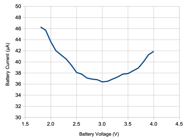
We eliminate support for random stimuli and for modulated stimuli. Software drops to 2800 bytes and firmware drops to 1242 LUTs. Tag P3054 with v1.5. Wash circuit board, dry, and allow to cool. Ripple with no activity is 10 mVpp. Measure wake state battery current versus battery voltage and plot. Measure 256 SPS transmit current versus battery voltage: rises from 238 μA at 1.8 V to 252 μA at 4.0 V. At 3.0 V, 241 μA. The transmit current is mostly that current consumed by the temperature sensor, which we have configured to run continuously as fast as it can. In the A3054X, the sensors, clock, and crystal radio are all powered by 1V8.
Disable the temperature sensor. Measure transmit current versus sample rate for five different signals: ACC, ADC, NVM, TEMP, and SYNC, for which we use channel numbers 11, 1, 10, 9, and 12 respectively. We have no accelerometer loaded, so sample cost is all in the logic and VCO. During SYNC we are not generating a stimulus. We measure the length of the interrupt service routine for each and get: 150 μs, 48 μs, 148 μs, 148 μs, and 44 μs respectively. In all cases, the VCO powers up for 8 μs.
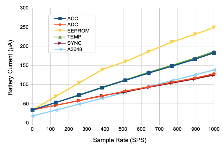
The slopes are ACC: 0.148μA/SPS, ADC: 93 nA/SPS, EEPROM: 212 nA/SPS, TEMP: 151 nA/SPS, and SYNC: 90 nA/SPS. We assume worste-case A3048 0.120 μA/SPS even though in practice the value for the A3048 is 100 nA/SPS. Because we have no ACC, and the SYNC is internal to the logic, the difference between the ACC and SYNC slopes is due to 106 μs per sample additional time for which the CPU is in boost mode for the ACC readout compared to the SYNC readout. The slope difference is 58 nA/SPS. Battery current due to boost is 58 nA-s/sample / 106 μs/sample = 550 μA. This suggests 1V2 current is 550 μA * 3.0 V / 1.0 V * 0.8 = 1.3 mA, which is close to the 1.2 mA we estimate in the OSR8 Processor Manual. The SYNC slope of 90 nA/SPS consists of 44 μs of boost and 8 μs of VCO. The 44 μs of boost generates 24 nA/SPS, so the radio-frequency transmit is consuming 66 nA/SPS. Given that the VCO is on for 8 μs, this suggests the transmission draws 8.2 mA from the battery. The NVM reads consume an additional 64 nA/SPS compared to the ACC reads, which are of almost exactly the same length. Each NVM read consumes 64 nC of charge. We examine SCL and see the NVM read takes 104 μs, so the read current is 610 μA. The data sheet says maximum 1 mA. The temperature sensor consumes only 3 nA/SPS extra with the same 104-μs readout time, so its read current is of order 30 μA. The data sheet says typical 15 μA at 400 kHz. We are running at 500 kHz. The ADC readout consumes 3 nA/SPS more than the SYNC while taking 4 μs more in boost. The 4 μs at 550 μA accounts for 2.2 nA/SPS. The remaining 0.8 nA/SPS is reading out the ADC, although at this point our resolution of ±2 nA/SPS is greater than our quantity.
When transmitting ADC samples, we have two dominant sources of current consumption: 66 nA/SPS for transmission and 27 nA/SPS for CPU boost. The ADC conversion and readout are negligible. The ADC read takes only 5 μs of the 48 μs of the interrupt. The rest is pushing registers onto the stack and figuring out what the interrupt should do, which we count up to be around 160 clock cycles, or 32 μs at 5 MHz, plus 8 μs for transmit is 45 μs total, which compares well to our measured 48 μs.
We set up a temperature measurement counter that decrements one each pass through the main loop. When zero, the interrupt routine detects the zero and initiates a one-shot temperature measurement. The communication with the sensor must run in the interrupt so it will go fast and so that it will not be interrupted by some other I2C access. With the counter set to 65 we get a temperature measurement every 55 ms. At 128 SPS transmit of ADC our current consumption is 100 μA, up from 46 μA. The 18 Hz temperature readout is costing us 54 μA. The TMP117 data sheet says 1 Hz is typically 3.5 μA. We would like to try updating every two seconds, so we need a two-byte counter, counting down from 0x0900. With this implemented, we see roughly 0.5 Hz update and current is 47 μA for ADC readout, jumping up to 60 μA occasionally during measurement. In temperature transmission at 128 SPS, current is 56 μA. We see the reading changing every two seconds in the Receiver Instrument.
We are measuring current consumption at about 23°C. We expect the static current consumption of the logic chip to increase by 8 μA at 37°C. Our implanted current consumption for ADC sampling and transmission will therefore be our existing 36 μA at 23°C plus 8 μA is 44 μA. The transmission cost is 8 μs * 550 μA = 4.4 nC of boost plus 66 nC for the VCO = 70 nC. To read out an ADC and accumulate we need 5 μs of boost, or 2.5 nC. The ADC takes another 0.5 nC. If we do this 1024 times per second we have 3.0 μA overhead for any enabled channel.
[27-MAY-26] We have in hand our A305401A Intraperitoneal Transmitter PCBs and our A305402B IPT Test Fixture PCBs. The A305401A rigid sections are 0.6 mm thick, the flex sections 0.13 mm thick. They come panelized 10 × 1. When we break them apart we sand two sides of each rigid section to remove perforations.
We construct the A3054TF IPT Test Fixture using the A305402B printed circtuit board. The test fixture allows us to connect an A3054AV1 IPT to power and programming. We load C1, U1, U3, Q1, U2, L1, C3, C2, U4, and U5 in stages on two boards, testing as we go using the A3054TF test fixture. We name the boards I and II. Program U4. Wash and dry. Quiescent current is 28 μA for I and 28 μA for II. Sleep current 0.8 μA for both.
[29-MAY-26] Current consumption for both boards today is 25 μA. We load all parts needed for the crystal radio, as well as the LED. Both boards now respond to stimulus commands by flashing their LED. Quiescent current consumption is 28 μA for I and 27 μA for II.
[02-JUN-26] Load U11 and DAC resistors. See TUNE and D0-D4 supporting transmission. Our calibration of the center frequency is for the A3054X in which the DAC is driven by 1V8, which no longer exists. Now the DAC is driven by VS, which is 3.0 V. Our frequency_low calibration was 24, which means we were seeing around 910 MHz for TUNE = 24 / 31 * 1.8 V = 1.4 V, which agrees with the MAX2623 data sheet. Now we are applying TUNE = 24 / 31 * 3.0 V = 2.3 V and we expect the low frequency to be around 980 MHz. Our spectrometer indicates the center is at around 1 GHz. We should move our calibration down to 1.4 / 3.0 * 31 = 14.
[03-JUN-26] We drop frequency_step from 2 to 1 and frequency_low from 24 to 14 and now obtain 100% reception from I and II. We have acknowledgement and transmission. Ripple on 1V2 during transmission is 12 mVpp in I and 18 mVpp in II. We measure specifically the range of 1V2 at the moment of transmission and find the same 12 mVpp and 18 mVpp ranges. We inspect he buck converter capacitors and inductors, as well as all joints on U2, but can see no difference between the two boards. We drive directly with our bench-top power supply and no longer see downward spikes in VS when U2 connects L1. But we still see 18 mVpp in II and 12 mVpp in I.
Load accelerometers BMA423 for U6 on both boards. We are configuring U6 for 100 Hz acceleration readout. Current consumption with no transmission is 46 μA for I and 48 μA for II. We read out x-direction acceleration and are able to generate sine waves by wiggling the test fixture. We disable the accelerometers in firmware on both boards and now see 28 μA in I and 29 μA in II. The accelerometer, when disabled, appears to draw only 1-2 μA. Load TMP117 temperature sensors. Quiescent current now 28 μA in I and 29 μA in II. No temperature measurements taking place. Turn on temperature transmission at 256 SPS with 0.5-Hz updates and current is 75 μA in I and 73 μA in II with brief jumps up by 10 μA every two seconds. Load M24C16 non-volatile memory. Attempt to initialize and read back the first sixteen bytes. We see 0x57 and 0xAA when we write them, but not where we expect them, and we see 0xFF. There is something wrong with our i2c routines. We confirm the temperature sensor and accelerometer are still working, for which we have to enable the accelerometer temporarily. Disable accelerometer. Write 0x00, 0x10,... 0xF0 to addresses 0 to 15 with eight-bit writes. When we read back two bytes from address 0 we see 0x0010, which is correct. Current consumption with NVM loaded, thermemoter inactive, accelerometer disabled, is 28 μA at 24.8°C for I and 32 μA at 25.0 °C for II. Our I2C bus appears to be complete and functioning.
[04-JUN-26] Current consumption this morning for I is 28 μA at 24.1°C, for II is 33 μA at 25.7°C. We warm up the circuits with a heat gun and cool them with freezer spray so as to vary their temperature. We measure temperature with 256 SPS temperature transmission and 0.5 Hz temperature measurement. The current jumps up by 10 μA briefly every two seconds as the temperature sensor makes its measurement. We take the lower battery current as our measurement of battery current. To measure temperature, we are using our new Temperature Gauge script.
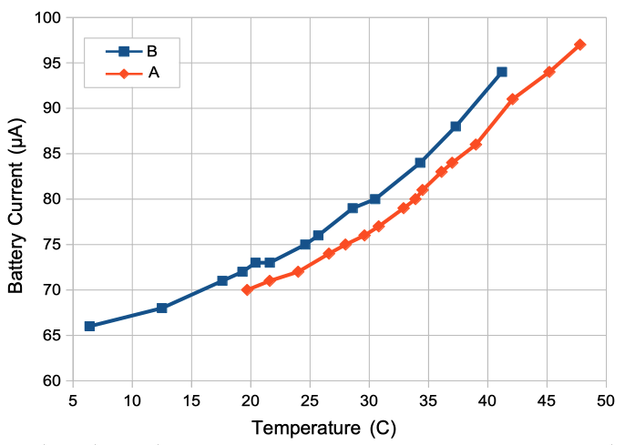
At 37°C, we turn of temperature transmission for circuit I and see 41 μA quiescent current, compared to 84 μA with 256 SPS. Current consumption of transmission is (84 − 41) / 256 = 168 nA/SPS for temperature sensor readout and transmisson. Quiescent current consumption at 37°C for circuit I is 41 / 28 = 1.46 times higher than at 24°C. For circuit II at 25.8°C, quiescent current is 32 μA. Turn on 256 SPS temperature and we see 76 μA, which is (76 − 32) / 256 = 171 nA/SPS. Turn on readout and transmission of non-existent ADC and we have 56 μA for (56 − 32) / 256 = 94 nA/SPS. On circuit I we increase to 512 SPS and we have 78 μA for (78 − 29) / 512 = 96 nA/SPS. We create a new transmission channel, one that transmits the device identifier rather than performing any readout. Now, for circuit I we have 51 μA at 256 SPS and 28 μA quiescent current, so our dynamic consumption for interrupt and transmission alone is (51 − 28) / 256 = 90 nA/SPS. Instead of reading out the temperature sensor 256 times a second, we read it out prior to initiating conversion every 2 s, and store the temperature in memory. When we transmit a sample, we read this saved value from memory. Now the temperature signal current consumption is 51 μA at 256 SPS. Cost of 256 SPS temperature measurement is 90 nA/SPS. From this we deduce that the cost of reading out the temperature sensor is roughly (171 - 90) = 81 nA/SPS. In circuit II, 256 SPS temperature now costs 54 μA.
We spend 45 minutes trying to load a single XDFN-4, in this case U16 TCR3UM, and fail. We were able to load these with no trouble using our SMT oven when we worked on the A3054X, so we apply paste and place U16, U17, as well as U14 and U15 on circuits I and II. When we apply paste, we smear it all over the pads. We don't try to just keep it on the pads. With extreme care and repeated attempts, it is indeed possible to restrict the paste to the pads, but when we place the part by hand, it will shake, and the paste gets smeared everywhere. So our only practical option is to apply a puddle of paste, not so much that it is spreading around, just enough that we can stick our part into the paste and have it stay where it is. Now we subject to reflow. Afterwards, we have solder bridges and solder balls, but we can clean all those up easily with our soldering bit. After clean-up, three out of four UDFN-4 are working. One we reflow and move around with our iron and now it is working. We have VA and VC on both boards. The XQFN-8 are almost perfect, but we have to use a sharp tip to complete two joints.
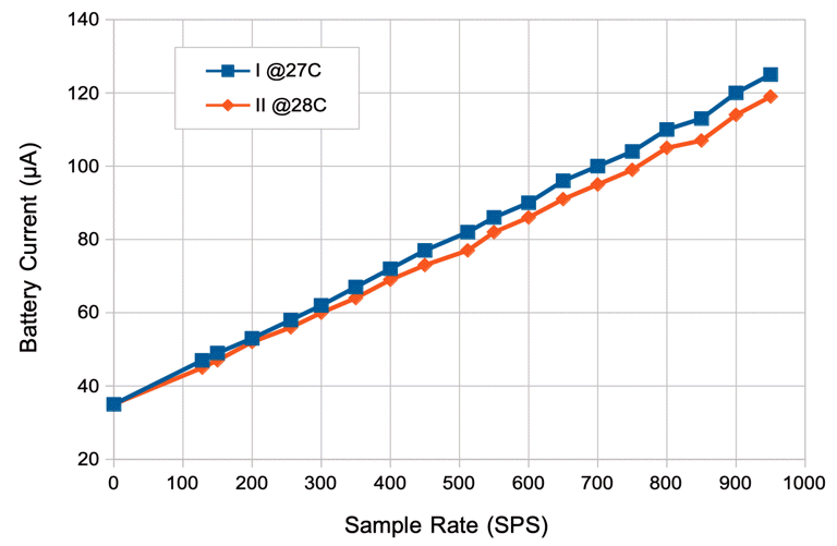
[05-JUN-26] Load all remaining parts onto circuits I and II, see A3054AV1. Decide to set the input impedance to 500 kΩ, for which we load 499 kΩ 1%. At 25.4°C, circuit I consumes 34 μA. At 25.5°C, circuit II consumes 33 μA. Check all four inputs with sweep and square wave, including switching X1-X3 from AC to DC. All perfect. Plot current consumption versus sample rate for X1.
Right now, our code is waiting about 20 TCK periods for the ADC conversion to complete, which is 4 μs. During this time, the OSR8 is in boost mode. We expect it to draw around 530 μA. For each sample we are consuming 2.1 nC of charge while waiting. This contributes 2 nA/SPS to the roughly 90 nA/SPS total sample cost.
Heat circuit I in oven, take out and measure curent consumption as it cools, then cools with blanket and freezer spray and measure current as it warms up. Heat circuit II in oven, take out and measure current consumption as it cools.
[08-JUN-26] Our three iEEG inputs, when configured with AC-coupling, are subject to a single-pole 160-Hz low-pass filter. When DC-coupled, the amplifier gain is less by a factor of four, and the low-pass corner frequency rises to 600 Hz. If we sample these inputs at 1024 SPS, we will be able to recover the shape of the original signal with a minimum of aliasing distortion, especially given that there is very little power in EEG over 160 Hz. In order to transmit the signals at less than 1024 SPS, we must combine samples in some way. We might add 16 14-bit samples and divide by 4 at the end to obtain a single 16-bit sample that we can transmit at 64 SPS. We want to perform these sample accumulations as efficiently as possible, which is to perform them directly in logic. We need four 18-bit accumulators, one for each ADC. We eliminate the stimulus code from our OSR8 program and VHDL. On stimulus start, the LED turns on and stays on. On stimulus stop, the LED turns off. Our OSR8 code is still 2430 bytes long, which means it overflows the main program area of 2048 bytes, so we are still disabling the user program. We extend our adc data register to eighteen bits and provide support for zero to four left shifts of this data before adding to an eighteen-bit accumultor. We do not yet have the accumulators running, but the left shifts are working.
We add all four 18-bit accumulators to our VHDL, so that each of the four ADCs has its own box filter that can be configured for summing between one and sixteen samples. The code consumes 1294 LUTs and we have only 1280 available. If we eliminate the box filter for X4, and instead allow X4 to be read directly from the adc, the code takes 644 of 640 registers. If we get rid of the cyclic redundancy check process, all four accumulators fit. Maybe we can do the cyclic redundancy check in software, but the command memory is a FIFO, so reading once for CRC and then again is impossible. Restore CRC and remove interrupt 4, but code still does not fit. Restor interrupt 4. Eliminate X3 and X4 accumulators, enable direct read of adc data. Code fits.
[10-JUN-26] Circtuit II now shows variable wake current and poor reception of commands. We remove U6 and current stabilizes at 35 μA. Circuit I has U6 loaded. Wake current is 35 μA. But in Circuit I we have an open circuit between P2-10 and X4N at J7, and an intermittent open circuit between P2-9 and X4P at J6. As a result, the X4 amplifier does not respond correctly to signals applied through the test board. We connect J7 to P2-10 and J6 to P2-9 with wires and X4 now responds correctly. To deliver a signal to the board, we provide power from a battery. We cannot tell if the A3054 is awake or asleep because we no longer have an ammeter in series with the power supply. We add a triple flash of the lamp to the initialization process.
We reduce the CPU's RAM space from 4 KB to 2 KB, which reduces the CPU address length from 11 to 10. We re-arrange the CPU memory map so as to allocate 256 bytes each to control registers, main program stack, user program variables, and main program variables. We allocate the top 1024 bytes to program memory. Our program memory, meanwhile, remains 4 KB with the upper 1 KB mapped into the upper 1 KB of the CPU memory. Now we have 3 KB for the main program, which is now 2500 bytes long. We restore support for the user program.
const ctrl_bot   0x0000 ; Control Registers
const stack_bot  0x0100 ; Main Program Stack
const uvar_bot   0x0200 ; User Program Variables
const mvar_bot   0x0300 ; Main Program Variables
const prog_bot   0x0400 ; User Program Instructions
const prog_top   0x07FF ; Top of Address Range
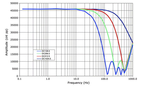
We have 1 KB of RAM, so we direct all writes to 0x0000 to 0x03FF to RAM, and when we read back from control registers, if their state was set by a previous write to the control register, we have a RAM shadow of the register. We eliminate some readback code from the memory manager, which saves logic, allowing us to restore direct access to the top sixteen bits of the eighteen-bit ADC data word. We drop the minimum transmit period to 7 RCK periods so that we can run at 2048 SPS. When sampling from an ADC and transmitting, our interrupt is taking about 42 μs. When in boost, the OSR8 and TCK consume 500 μA from the battery, so our logic current consumption is 500 μA * 42 μs = 21 nA/SPS. At 1024 SPS we get 100% reception, and at 1600 SPS. But higher than that, we don't get any more samples per second. We are marking our interrupts with df_reg(0). When our oscilloscope claims these pulses are occuring at 2.05 kHz, we are seeing only 1300 SPS received, both with ODR and TCB. We set up the ADC readout to shift left twice and we accumulate four samples in our eight-bit accumulators. Every four interrupts we transmit a sample. We are now able to measure the frequency response of our digital box filter on top of the op-amp bandwidth filter. We set up the software so that it always samples at 1024 SPS, and if we ask for 128, 256, 512 or 1024 transmitted samples per second, it obliges us, and applies a box filter to the 1024 SPS signal with width 8, 4, 2, and 1 sample. Working for AC, then find obvious bug in DC and correct but do not test, tag v1.9.
[11-JUN-26] We test P3054 V1.9 and find its box filters working perfectly for all channels and both AC and DC. We add some plots to "Frequency Response for Various Sample Rates". We have been using Circuit II, but now we switch to Circuit I and program it with the new code. This is the circuit with two wire linke repairs on it. We plot the AC and DC frequency response of the X1 amplifier with 128 SPS, for which we are using an eight-point box filter.
[12-JUN-26] We recruit the final EBR block in our logic chip as a sample memory and arrange it as 256 x 14 bits. We store fourteen-bit ADC samples in this memory, with a separate space for each of the four ADCs. We do not accumulate during sampling, but instead accumulate at transmit time. We multiply each sample by adding it multiple times to the accumulator, and so obtain a sum that occupies the top sixteen bits of the eighteen-bit accumulator output. Whith transmit period 1, we have 1024 SPS transmitted, and we add the single sample sixteen times, which takes 16 μs. With transmit period 8, we have 128 SPS transmitted, and we add each of eight samples twice, which takes 36 μs. With these changes, our code drops from 1250 LUTs to 1120 LUTs out of 1280. We are using only 568 SLICEs out of 640. We commit our updated firmware and tag v1.10. Right now, our accumulation takes time because it is executed by the code below. But we now have enough gates to automate the accumulation so that it will take no more than 20 TCK periods, or 4 μs.
int_xmit_acc_loop:
  push
  pop A
  ld (IY),A
  push E
  pop D
  ld A,sm_add
  int_xmit_mult_loop:
    ld (IX),A
    dec D
  jp nz,int_xmit_mult_loop
  inc B
  dec C
jp nz,int_xmit_acc_loop
We check the X1 input with all sample rates 128, 256, 512, and 1024 SPS with AC and DC coupling, measuring and plotting sweep response. We obtain the same results as before. We are satisfied that our binning and multiplying is working.
We measure noise in counts directly from the Receiver Instrument's standard deviation ouput. We do not filter before-hand, and we use one-second intervals, so we are looking at total noise. We convert noise in cnt rms (counts root mean square) to microvolts rms using the dynamic range 112 mV for the DC input and 30 mV for the AC input. With 256 SPS and AC input, our noise is 2.8 μV rms, which roughly half amplitude we see with an A3048R2.
| Sample Rate | DC (cnt) | AC (cnt) | DC (μV) | AC (μV) |
|---|---|---|---|---|
| 128 | 3.4 | 4.4 | 5.8 | 2.0 |
| 256 | 4.8 | 6.1 | 8.2 | 2.8 |
| 512 | 6.1 | 8.2 | 10.4 | 3.8 |
| 1024 | 9.4 | 10.5 | 16.1 | 4.8 |
The A3054 noise signal contains no random positive spikes nor extended quantization artifacts. In the A3047, A3048, and A3049 devices, we read out samples during the transmission period, which is scattered randomly with respect to the start of each transmit period. We cause another conversion at the beginning of each transmission period, and the variable spacing between the conversion and the readout causes spikes. Here we are sampling and reading out at the start of every sample period, which is 1/1024 s. We are storing the result in our sample memory, and we do not read the ADC out again until the next regular sample time.
[19-JUN-26] We prepare a new LWDAQ tool, the Telemetry Manager, which does away with the stimulator functions and replaces them with Lon, Loff that just turn the lamp on and off. We add Zon and Zoff to turn on and off the impedance measurement function. For these functions we add four new operation codes. We update P3054 accordingly. We connect a battery to circuit I and turn on channel X1 with DC coupling. Average value is 32975 cnt, random noise amplitude 6.5 cnt rms. We execute the Zon and average value drops to 28865 cnt, noise jumps to 18 cnt rms and is dominated by 60-Hz hum. The drop is 4110 cnt = 112 mV * 4110 / 65535 = 7.02 mV. We have the circuit plugged into our A3054TF IPT Test Fixture. The DIN and CIN inputs are open circuit. Both DIN and CIN are connected to ground through 51 Ω on-board. On the test fixture, X1-X3 connected through 1.0 kΩ to ground and 100 kΩ to DIN, which is also ground. Within the circuit, we have GND moved from VC downto VC −7.14 mV, which moves VC up 7.14 mV with respect to ground, and our grounded inputs appear to go up by 7.14 mV. Within the circuit, X1-X3 are connected to their amplifiers through 1.0 kΩ and then 500 kΩ connects the amplifier input to VC. So the −7.14 mV drop appears as 500 / 502 * 7.14 mV = 7.11 mV across the 500 kΩ. Our hope is that if we loaded 10 kΩ on the test fixture for R4, we would see a step of order −700 μV on X1.
[22-JUN-26] Using Zon we apply a 7.14 mV negativer step to GND. In our test fixture, with the CIN and DIN inputs open-circuit, both X4P and X4N are connected to GND through 1.0 kΩ on the fixture. We cannot measure electrode impedance, but we can measure common-mode rejection ratio (CMRR). With Zoff and 512 SPS the average X4 is 32712 cnt with 6 cnt noise. With Xon, X4 drops to 32685 cnt and noise remains 6 cnt. That's a drop of 27 * 90 mV / 65535 = 37 μV for a common-mode drop ot 7.14 mV for CMRR of 46 dB. We increase sample rate to 1024 SPS and apply the same 10 Vpp sinusoid to both DIN and CIN, so that 100 mVpp will be applied to both X4P and X4N. We measure the amplitude of our X4 signal versus frequency using our SCT Check tool. The X4 response to the sweep peaks at 100 Hz with an output of 340 μVpp, which is a CMRR of 340 μV / 100 mV = 49 dB.
The maximum common-mode signal we expect to see between GND and X4P/X4N is around 10 mV, where we have massive iEEG spikes during seizures. A 10-mV common-mode spike will appear as a 34 μV spike on the X4 signal due to the intrinsic CMRR of our amplifier. In practice, the electrode impedances stand in between the signal source and the amplifier, adding to the values of the two amplifier input resistors. Suppose the electrode impedances are 1 kΩ, as we might hope for a 1-mm coil of wire sewn into a muscle. They might easily be mismatched by 200 Ω, which is 0.1% of the 200-kΩ input resistance of the X4 amplifier. This effect along gives us 60 dBm CMRR, which is still better than the intrinsic CMRR of the amplifier. We consider purchasing 0.1% 100 kΩ and 2.0 MΩ resistors, but we cannot find 0.1% 2-MΩ resistors, an in any case, we cannot expect 2.0 MΩ resistors to remain stable to 0.1% during weeks of implantation. We will have to be satisfied with CMRR of around 50 dB.
We restore the cyclic redundancy check to the firmware. We had previously removed it to save logic. Now we see the LUT consumption rise from 1122 to 1143, still well below our capacity of 1280. All commands are now guaranteed error-free prior to being passed to the OSR8. We reduce our I2C library to two routines: a write and a read. We can read up to 256 bytes with one call to the read routine, and we can write the same with the write routine. We use IX to point to a the location to which data should be transferred to or from and we use C as a counter. We create a scratchpad for data transfers. Our asssembler code drops from 2850 bytes to 2320 bytes. We distribute the start-up flashes throughout the initialization sequence so that if we do not get three full flashes, we know roughly where the initialization has failed. We use these flashes to debug our new I2C routines. We move the routines back into ROM.asm, attaching them to the end. Quiescent current at 27°C is 33 μA in circuit II. We now have Lon/Loff, Zon/Zoff and compact general-purpose I2C in P3054 V1.11.
We break out the I2C routines again. We include I2C.asm and the eight-bit multiplier in the OSR8 repository, M8X8.asm. Our code is now 2387 bytes, still well below the 3072 maximum. In order to make a scalar accelerometer activity measurement at 1 Hz, we can calculate the scalar value in the main loop, which runs at 32.768 kHz without the fast clock current consumption. Each eight-bit multiply takes about 8 ms. The acceleration values are twelve bits, so we use four eight-bit multiplies to produce a twenty-four bit result. We add three of these together to form a thirty-two bit result, then take the square root using the restoring binary square root algorithm. We can get all that done in 200 ms with no overhead in current consumption. The interrupt routine read a new x, y, and z value from the sensor when it sees an acquisition flag is set. It also reads the activity value provided by the main loop and makes a copy for its own use. Now the interrupt routine clears the acquisition flag. The main loop goes about calculating the new activity value, which it eventually writes to memory, at which point it sets the activity flag. Meanwhile, the interrupt routine has been transmitting the previous activity value from its copy at 32 SPS.
Instead of having the Telemetry Manager adjust the telemetry protocol in small steps, we will have it upload a configuration record to the A3054, which will then be written to NVM in the first 1 KByte, and after that, we re-boot the A3054. Initialization looks for a special code at the start of NVM, which indicates a valid configuration, and a code at the end. The configuration sets all the configuration bytes of the telemetry protocol. After initialization, the A3054 always enables the telemetry protocol. We can turn it off and on with Xoff and Xon. Also during initialization, the A3054 reads the second kilobyte out of NVM and puts it in the user program area. We can enable and disable the user program with Pon and Poff. The A3054 never starts running its user program when it powers up. We must use Pon. When we upload a new user program, the command receiver writes the new program to NVM and then the Telemetry Manager re-boots the A3054.
[24-JUN-26] We configure the accelerometer in circuit I for 100 Hz update and read out the twelve-bit x-value and transmit at 1024 SPS. Battery current 228 μA. Turn off transmission, current is 52 μA. Accelerometer readout and transmission costs 0.17 μA/SPS. Within the accelerometer, 100 Hz update costs only 52 - 33 = 19 μA. We reduce the accelerometer update rate to 1 Hz. We examine this signal. It does not appear to be taking averages, but rather it samples the accelerometer once per second. Such sampling is suitable for measuring activity in animals. Current with 1024 SPS is 210 μA, and when we turn off 34 μA at 24.9°C. The cost of sampling at 1 Hz appears to be negligible. We program circuit II, which has no accelerometer loaded. Current consumption with no transmission is 34 μA at 25.7°C. With 1024 SPS accelerometer we have 207 μA. We load a BMA423 onto circuit II, but we cannot get it to respond. This is the third of fourth BMA423 we have loaded onto circuit II without success. We find a break in the VB flex track and replace with wire link. So far, three flex tracks have broken due to fatigue as we play with these two circuits.
[29-JUN-26] We are curious to know if we could run the A3054 circuit with an LCMXO2-256 in the same package. This smaller version comes with no embedded RAM blocks, so we would have to make our program memory and process memory out of LUTs. We strip the OSR8 down to instructions that use only A and B, allowing "ld A,B" and "ld A,(nn)", but removing index registers, to create a minimal processor with no subroutine calls, but supporting interrupts and with a stack. We drop RAM and program size to 256 bytes. We remove the command receiver. We remove direct read of ADC outputs, but keep the sample accumulator. Code size drops to 600 LUTs. Remove support for interrupts, code size drops to 480 LUTs. Maximum CK frequency remains 8 MHz with 16 levels of logic. This is still far from 256 LUTs, and we do not even have the program and process memories in LUTs yet, they are still in EBRs.
If we are to run the A3054 with 256 LUTs, we cannot do so with a CPU. But we could build a command receiver that detected two specific commands: Xon and Xoff with the device's ID, and we could construct four ADC sample accumulators and a firmware I2C interface for the temperature sensor and NVM. The configuration would be fixed at the time of calibration. The transmitter would turn on with a magnet and start transmitting. We could deactivate and activate by radio command. Quiescent current would be around 20 μA. If we eliminated the crystal radio, accelerometer, and temperature sensor, but kept the EEPROM, quiescent current consumption would drop to around 10 μA and we could keep a record of charge consumption in the EEPROM to settle questions of premature failure.
In P3054, we eliminate the user program memory. We provide the CPU with a 4-KByte ROM that cannot be re-written aside from by re-programming the chip. Code size drops to 1096 LUTs from 1148 LUTs. We remove user program support from the software. We re-purpose the user program upload for writing to the NVM. We alter the Telemetry Manager to read in a file of byte integers and write them in 32-byte chunks to a specified address in the NVM. This works only if the address we supply is on a sixteen-byte boundary. We write sine waves to the entire 2 KByte memory. We turn off power, turn on again, and the sine waves are still there.
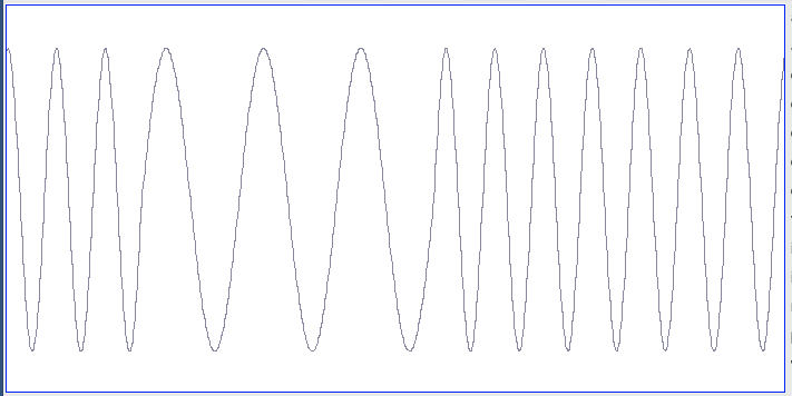
[02-JUL-26] We have all four inputs being sampled at 1024 SPS. At 256 SPS we add each of four samples to our accumulator four times to give an answer from which we can take the to sixteen bits as our sample. We have the accelerometer updating at 100 Hz and being read out and transmitted at 128 SPS. The temperature sensor we read out every second and transmit at 32 SPS. The NVM we read out at 1024 SPS. Our Telemetry Manager uploads data to the NVM in blocks of 16 to 256 bytes. We can watch the NVM signal changing as we upload new blocks of bytes to the NVM. Current consumption is 379 μA from 3.0 V. Disable accelerometer update, readout, and transmission. Disable temperature sensor readout and transmission. Disable NVM readout and transmission, leaving 4 inputs at 256 SPS. Current consumption is 199 μA. When we turn off transmission, inactive current is 36 μA. Dynamic current is 163 μA, or 160 nA/SPS. We recall from 05-JUN-26 that simply reading a sample from the ADC and transmitting it without accumulation costs roughly 90 nA/SPS. Now that we are taking four samples for each sample transmitted, accumulating the four samples, and shifting them two places to the left by adding each four times to the accumulator, we consume 70 nA/SPS more current. Instead of 32-μs interrupts at 1024 SPS we now observe 83 μs interrupts at 768 SPS and 275 μs interrupts at 256 SPS. The former when we add four new samples to memory, the latter when we add four samples and then accumulate and transmit. We are spending 110 ms more time in boost mode with the accumulation process. The oscillator and CPU alone consume roughly 500 μA from the battery, and so the extra boost time accounts for an extra 110 ms * 500 μA = 55 μA, or 54 nA/SPS.
Of the 70 nA/SPS additional current consumption, we appear to be able explain 54 nA/SPS as extention of our interrupt duration. The remaining 16 nA/SPS may be due to the accumulator. The eighteen-bit accumulator adds each of 4 samples 4 times for each of 4 channels 256 times a second for a total of 16k additions per second. Each accumulator consists of 30 LUTs. If each addition causes 2 transition per LUT we have 2 * 30 * 16k = 100k transitions per second, which is like 50 kHz. The current consumption of the logic gates from the battery is roughly 460 nA/MHz. The accumulators could easily be using 50 kHz * 460 nA/MHz = 23 nA. We must reduce the interrupt durations and the accumulator usage if we want to get our dynamic consumption below the 110 nA/SPS of the A3049 circuit.
[03-JUL-26] We would like to avoid repeat addition in the accumulator to generate left shift. We increase the width of the sample memory to eighteen bits, add an accumulator shift value acc_shift in the range 0-4, and use this to generate shifting of an eighteen-bit sample in the Sample Controller. Logic size increases from 1096 to 1134 in our first try, and then with the shifting performed on values of the Sample Controller state, the code size drops to 1102. We also try performing the shift when reading from the accumulator output, using acc_shift to control a multiplexer of the accumulator bits, but this increases logic size to 1170 LUTs.
We improve the efficiency of our interrupt code by polling ADCBSY and TXA before sample and transmit rather than waiting after each sample and transmit for ADCBSY and TXA to be un-asserted. Quiescent current today is 36 μA. Starting up four channels at 256 SPS, current consumption is 184 μA. Our interrupts are 80 μs and 180 μs. Reception with nearby antenna is exactly 256 SPS. We try the same telemetry protocol, but with no shifts in the Sample Controller, so we are avoiding 2 shifts/sample * 1024 SPS * 4 channels = 8192 shifts/s. Current is now 180 μA. Our shift cost is of order 4 μA / 8192 = 0.5 nA/shift/s. We restore the shifts. We disable adding to the accumulator, thus avoiding 4 * 1024 SPS = 4098 additions per second. Current is 181 μA. The cost of the additions appears to be 0.7 nA/add/s. Restore accumulation, eliminate Sample Controller reads, so we stop the Sample Controller from doing anything and we stop the ADCs being read out. Current is 175 μA. Restore all functions and disable transmission. Current is 108 μA. Interrupts remain 80 μs and 180 μs. Restore all functions and set all four channels to 1024 SPS with a shift of four places left for each sample. Current is 423 μA with all interrupts 136 μs. Disable X2-X4 so we have X1 at 1024 SPS. Current is 155 μA, interrupts 66 μs. Disable all transmit channels, current with Ton is 66 μA and interrupts are 44 μs. We direct CK to TP so we can see when the CPU moves out of boost. We see CK = TCK = 5 MHz for 46 μs. We direct TCK to TP1 and see it turning on for 47 μs.
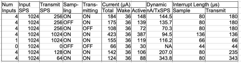
With 36 μA quiescent current today and 66 μA with the sample interrupt running at 1024 SPS but no sampling or transmission taking place, the cost of the interrupt is (66 − 36) μA / 1024 int/s = 29 nA/int/s. The interrupt lasts for 44 μs and our CPU is in boost for 46 μs. Our logic consumption in boost is 30 μA / 1024 int/s / 44 μs = 640 μA. Compare to 530 μA estimate presented in the OSR8 Manual. Consider the telemetry protocol with 4 channels being sampled at 1024 SPS and being transmitted at 256 SPS. We observed the total current consumption of this protocol to be 184 μA. We estimate that the boost-mode current for this protocol is (80 μs * 3 + 180 μs) * 256 SPS * 640 μA = 69 μA. The transmission current is 4 * 256 * 74 nA/SPS = 76 μA. The sampling current is 4 * 1024 * 2.1 nA/SPS = 9 μA. The quiescent current is 36 μA. Adding these together we get 69 + 76 + 9 + 36 = 190 μA, close to the 184 μA we observe.
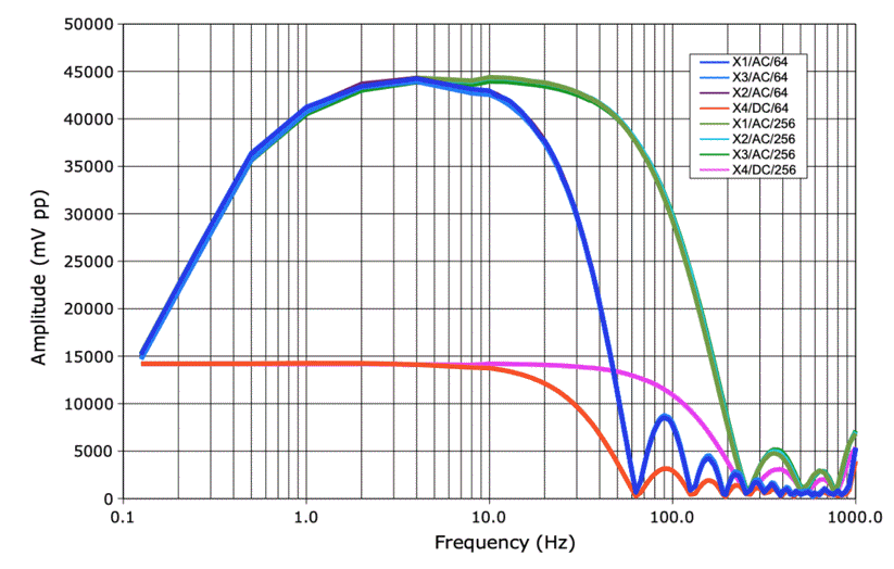
The overhead of putting the CPU into interrupt is 36 μA. We must eliminate the sampling interrupt. The sampling must be performed by logic 1024 times a second. The transmit interrupt will occurr at the frequency of the channel with the highest transmit sample rate. We see for the first time that we need a sample memory of only four locations of eighteen bits. Instead of feeding the accumulator output back into itself, we feed the output of the sample memory into the accumulator. Now we are accumulating in the memory. When it comes time to read the sample for transmission, it will already be prepared. We implement this idea in P3054 V1.13. The new system works well, except that we are not yet resetting the accumulated value after transmission, so the output keeps climbing. Current consumption with 4 channels transmitting at 256 SPS is 165 μA. Interrupts are 67 μs sampling-only and 98 μs for sample-and-transmit. Compared to our V1.12 code, the reduced interrupt times suggest a reduction in current of (13 μs * 3 + 82 μs) * 256 * 640 μA = 20 μA, which compares well with the 19 μA we observe.
[04-JUL-26] For each 10 μs of sample interrupt, we consume 10 μs * 640 μA * 1024 SPS = 6.6 μA from the battery. For each 10 μs of transmit interrupt at 256 SPS, we consume 10 μs * 640 μA * 256 SPS = 1.6 μA. A sample interrupt that does no sampling takes 44 μs and one that reads and accumulates 4 samples in V1.13 takes 67 μs, so reading and accumulating takes 23 μs, or 15 μA. The other 44 μs consumes 29 μA, and this is our sampling interrupt overhead. We would like to eliminate this overhead. If we perform the read and accumulates with a state machine rather than an interrupt, we might use only 150 μA for FCK for 23 μs at 1024 SPS, which would be 3.5 μA, compared to a total of 67 μs * 640 μA * 1024 = 44 μA.
Suppose we have a telemetry protocol enable flag the CPU can set. When set, a firmware state machine, the Telemetry Manager, starts running off RCK, counting 0-31 for 1024 Hz. In state zero, the Telemetry Manager asserts SCRUN (Sample Controller Initiate) and enables FCK. The SCRUN signal starts the Sample Controller, which runs off FCK. The Telemetry Manager assumes that the Sample Controller will complete its tasks before the next rising edge of RCK. It proceeds through its states until it gets to the state whose numerical value equals that of tx_scatter, a four-bit random number seeded by the transmit sample least significant bit. This random value provides the transmission scatter required by our telemetry system. Having arrived at this randomly-selected state, the Telemetry Manager checks a counter to see if a sample transmission should occur in this 1024 Hz period. If the maximum telemetry sample rate chosen for all sensors is 256 SPS, a sample transmission will occur every four 1024-Hz periods. When the time for transmission arrives, the Telemetry Manager sets the transmit interrupt, which is int3.
The CPU services the transmit interrupt, int3, and clears the int3 bit when it is done. The CPU decides which sensors are due for transmission. One will always be due: the quickest one. All sensors due for transmission will be transmitted in the same interrupt. The sm_addr is set by the Sample Controller when SCBSY is set. The CPU cannot read samples while the Sample Controller is running. The CPU reads out the accumulated samples for transmission. The CPU can also assert ACCRST and SMWRCPU, which allows it to reset the Sample Accumulator output register and write the accumulator output to the Sample Memory, thus clearing the accumulated sample in memory.
The Sample Controller needs only one piece of information about each of the four inputs X1-X4 to obtain four samples, and that is the value of acc_shift it requires. These values the CPU has set in three-bit registers ready for the Sample Controller to consult. The Sample Controller starts by setting smem_addr to 00, acc_shift to the value for X1, and asserting ADCRD. It waits until it sees ADCBSY, then !ADCBSY, sets smem_addr to 01, acc_shift for X1, and so on, until all samples have been obtained and accumulated in the sample memory. It waits until SMGI is unasserted and returns to its rest state. In order to save current, we can reserve acc_shift = "111" to mean "skip". We might also find a way to turn off FCK when the Sample Controller is done, but having a state machin turn off its own clock is tricky. For now, we assume FCK will run for 30 μs and all of X1-X4 will be sampled. We will be consuming around 5 μA for sampling all four inputs at 1024 SPS.
With these machines in place, our transmit interrupt takes 40 μs plus 15 μs per X1-X4 channel transmitted. We are setting aside for now the use of the accelerometer, thermometer, or NVM reporting. At 37°C we have 40 μA quiescent current. At any temperature we have 5 μA sampling current. If we have X1-X4 transmitting at 256 SPS, the cost of the RF transmission is 74 nA/SPS * 4 * 256 = 76 μA. The cost of the transmit interrupt is (40 μs + 4 * 15 μs) * 640 μA * 256 SPS = 16 μA. Total is 40 + 5 + 76 + 16 = 137 μA. Compare to the A3047A2C 4 x 256 SPS iEEG monitor's maximum current consumption of 153 μA.
The transmit interrupt itself is straightforward when handling only X1-X4. We could manage such an interrupt with another firmware state machine. We would like to know if we can run the A3054 circuit with an LCMXO2-256ZE. This device has 256 LUTs with no embedded RAM blocks. We create a Lattice Diamond project for the LCMXO2-256ZE in the QFN-32. We carry over Main.vhd from P3054. We remove the CPU and associated logic. For the command memory, we substitute a sixteen-byte shift register for now. We retain the transmitter and the ADC sampler. Size is 124 LUTs. We add a 4 x 18-bit sample memory in distrubuted RAM, an 18-bit adder, and some code to make sure all these things are retained by the compiler. Size is 160 LUTs. The Telemetry and Sample Controllers will take no more than 15 LUTs each. A Transmit Manager will take no more than 20. We should still have 50 left to build an I2C interface that the Transmit Manager can use to read out the thermometer, accelerometer, and NVM. The LCMXO2-256ZE data sheet quiescent current is 15 μA compared to 56 μA for the LCMXO2-1200ZE. As it is, the LCMXO2-1200ZE draws 30 μA from our battery at 37°C, so we expect the smaller part to draw 15 / 56 * 30 μA = 8 μA, or 22 μA less. So our A3054 with smaller logic chip providing X1-X4 at 256 SPS might consume only 115 μA, probably less, because the Transmit Manager will be more efficient. Providing X1 only at 256 SPS, current would be around 47 μA, which is equal to that of the A3048S2.
[05-JUL-26] We add output registers to the accumulator and reset these to zero with ACCRST. We can cause a write to the sample memory with either SMWRADC from the ADC Controller, or with SMWRCPU, from the CPU. We use SMWRCPU after ACCRST to clear the accumulated sample pointed to by smem_addr. With the reset and stores included in our transmit interrupt, we now have X1-X4 correct. The sample interrupt has expanded to 73 μs. The transmit interrupt is 117 μs. Current consumption is 169 μA. Clean up comments and tag v1.13. Logic size is 1109 LUTs. We are using all 7 EBRs.
We start building the Sample Controller. We begin by having SCRUN asserted by the CPU with a write to the Sample Memory Control Register. We place this operation after pushing the registers on the stack in the interrupt routine. We look at SCBSY and two of the ADC select lines. The Sample Controller takes four samples, shifts, and accumulates in 19 μs. Each ADC is read out in around 4 μs. We have all four channels running perfectly. Logic size has grown to 1174 LUTs. The sample and sample+transmit interrupts are 50 μs and 100 μs respectively. Current consumption is 157 μA. Our expectation is (50 μs * 3 + 100 μs) * 256 SPS * 640 μA + 4 * 256 SPS * 74 nA/SPS + 36 μA = 153 μA, which suggests that the Sample Controller and its subservient ADC Controller are consuming 4 μA. Our next step is to eliminate the sample interupt, at which point we are hoping the current will drop to 4 μA + 100 μs * 256 SPS * 640 μs + 4 * 256 SPS * 74 nA/SPS + 36 μA = 132 μA. At 37°C this will rise to around 136 μA. Compare to the A3047A2C's 153 μA maximum. If we compare to the A4049
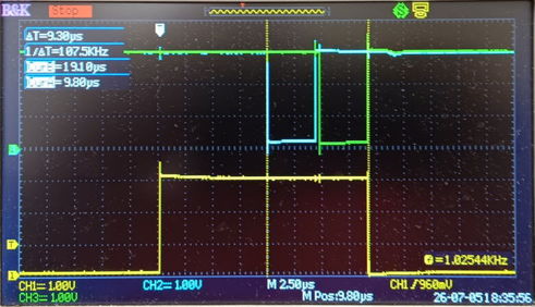
[06-JUL-26] We start building the Telemetry Manager. Our logic grows to 1230 LUTs. Our fast clock calibration is disturbed when we remove "syn_keep" and "no_merge" from the oscillator enable signals. Our TCK period rose as high 260 ns, which drove telemetry reception to 50% and 0%. We equip the Telemetry Manager with an index and period for each of X1-X4 to determine how often the signal should be sampled and accumulated in the Telemetry Manager cycle of 32 periods of RCK. We write the period from the CPU. If 0, the ADC is skipped. If 1, sample once per cycle. If N > 1, sample once every N cycles. The period allows us to disable the digital low-pass filter when recording chaotic, high-frequency signals like EMG.
We have the Telemetry Manager running when we set int_mask(0). It sets int_bit(0) to invoke the transmit interrupt. We have 256 SPS transmit now on all four channels, 100% reception because we were lucky guessing fck_divisor. Code is 1226 LUTs. We are adding the X1 sample to its accumulator only 3/4 of 1024 SPS (749 Hz on scope). Our received signal is 32767 or less, with quantization of 8192 cnt. Current is 134 μA.
[07-JUL-26] We eliminate the sample index and period in the Telemetry Manager for X1-X3 because we will never use them: the sampling of a chaotic signal will be useful only on the bipolar X4 input, and in that case we either accumulate all input samples between transmissions or we use only one sample between transmissions. So we use a flag X4SS for Input X4 Single Sample. We fix a bug in our Sample Controller. We now reset the Sample Controller with !SCRUN and otherwise it runs from its idle state to its wait state when FCK is running. All four channels working, check frequency response at 256 SPS. Wake current today is 33 μA. Active current is 139 μA. Our TCK is 213-225 ns, reception 100% with our ODR. Logic is 1179 LUTs. Transmit interrupt is 109 μs at 256 SPS. All channels being sampled at 1024 SPS.
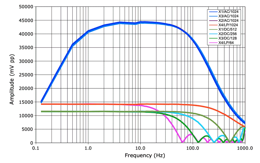
The transmit interrupt consumes 109 μs * 640 μA * 256 SPS = 18 μA. Transmission costs 74 nA/SPS * 4 * 256 = 76 μA. Quiescent current is 33 μA. So the sampling current is 139 − 18 − 76 − 33 = 12 μA. Per sample, that is 12 μA / 1024 / 4 = 2.9 nA/SPS. With transmit rate 1024 SPS per channel, we predict 74 nA/SPS * 4 * 1024 SPS = 303 μA for tranmission, 12 μA for sampling, 33 μA quiescent, and 109 μs * 640 μA * 1024 SPS = 72 μA for the transmit interrupt for a total of 420 μA. We re-program for 1024 SPS per channel and measure 418 μA.
[08-JUL-26] We are trying to make a software-programmable ring oscillator. While trying to debug our code, we enable FCK continuously and direct to TP1. When we do this, logic size shrinks from 1202 LUTs to 965 LUTs. Although the fast clock is included in the netlist, no fast clock nets are present in the floor plan: the fitter has eliminated them all. If we instead direct FCK to TP1 in place of df_reg(0), and allow the firmware to enable and disable FCK as usualy, our code is 1180 LUTs. Our savings of 22 LUTs is due to getting rid of df_reg(0). The oscillator remains in place. We set up the oscillator so that it uses an eight-bit mask we can write from the CPU. The mask selects which of the final eight gates in the ring we will be using to generate the feedback. With the mask set to 0x08, our TCK period is 177-189 ns, 0x10 gives 200-212 ns, and 0x20 gives 210-222 ns. In each test we re-assemble our source code but make no change to the firmware.
We implement reading from the NVM a 16-byte block into the scratchpad of the CPU. The first two bytes must match the calibration key. The subsequent bytes provide the device identifier, the fast clock (FCK) mask, and the RF calibration. The device identifier we now store in memory. We write to the bottom sixteen bytes of NVM using the Telemetry Manager's device programming panel. We turn off power, turn on power, and now we have the new calibration in place. We increase the FCK mask from 0x01 to 0x80 and measure the period of TCK. We have a total of 24 gates in the ring. For each mask value, the period of TCK varies by around ±5 ns. We put cursors at either extreme and take the average.
[09-JUL-26] We eliminate the Loff and Lon commands and replace with Flash. We try out the X4SS single-sample option for the X4 input. We seep from 0.0 to 1000 Hz and measure amplitude of the un-filtered X4 signal, which is being sampled at 64 SPS. We see its response following that of the 1024 SPS sweep. The shape of the sinusoid is lost above 32 Hz, but its amplitude is preserved.
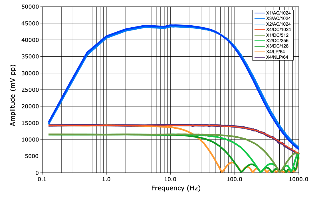
[10-JUL-26] Add to P3054 a reset instruction that we can use to follow upload of new calibration. P3054 V1.16 checks for invalid ID and FCK mask. There are eight valid masks, and we check for every one of them. If we were to write a bad mask, we believe it is possible for the fast clock to glitch and freeze the processor. Add configuration upload and deployment with correct configuration key in first two bytes. We transmit on X1-X4 at 512, 256, 128, and 64 SPS, with the X4 performing no accumulation. Active current is 135 μA. Wake current today is 33 μA. Frequency response as in the V1.15 plot above. We are now able to change the telemetry protocol by writing to the configuration block of the NVM. We define calibration and configuration with calib.txt and config.txt. Each contains a list of byte values to write to the calibration and configuration blocks, which are at 0x0000 and 0x0100 in the NVM respectively. Add acknowledgement of reset instruction.
We typed 0x030 instead of 0x030B for the address of the dc_in configuration variable. As a result, when we wrote to dc_in, we wrote to address 0x0030, which wraps to 0x0010 in the control space, and that is the fast clock mask. As soon as we wrote a zero, the fast clock would stop. Once we have that fixed, we note that samples are being dropped or corrupted when we have all channels running, and this turns out to be because the transmit interrupt can be as long as 380 μs when we transmit temperature, acceleration, NVM, and X1-X4, with X1-X4 at the end.
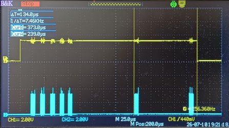
If the transmission scatter value was 15, the interrupt would begin in Telemetry Manager state 16 and X4 would be transmitted in state 27 or 28, while sampling was occuring in state 27. We put X1-X4 at the start of the interrupt. We move sampling to state 29. The seven-signal interrupt is shown above. Our signals are now undisturbed by collisions with the Telemetry Manager.
We have our calibration bytes recorded in Calib_10JUL26 and our configuration bytes recorded in Config_10JUL26. We write the calibration to NVM address 0x0000 and the configuration to address 0x0100. If we get them the wrong way aroung, the A3054 ignores them because they have different keys. We adjust and upload these a dozen times, looking at different combinations of inputs. We tag P3054 V1.17 all functions working.
[13-JUL-26] We adjust P3054 so that the device starts running its telemetry protocol as soon as it wakes up. With 4 x 256 SPS X1-X4, nothing else enabled, active current is 139 μA in circuit I. The transmit interrupt is 89 μs, suggesting 89 μs * 640 μA * 256 SPS = 15 μA of transmit management current. We expect the VCO to consume 7.4 nA/SPS * 256 SPS * 4 = 75 μA. Quiescent current 34 μA. That leaves 15 μ as the sampling cost, or 3.7 nA/SPS. According to the ADS7052 data sheet, ADC itself uses only 0.5 nA/SPS. Our sample management costs 3.2 nA/SPS. We adjust P3054 so that we run FCK during the Telemetry Manager sample state only so long as the Sample Controller is not done with its tasks. This drops consumption to 137 μA, but breaks the sampling. Nevertheless, we see that FCKENTM (Fast Clock Enable from Telemetry Manager) is asserted for 22 μs rather than 30 μs. The 8 μs reduction saves us 2 μA, which means FCK costs us 2 μA / 1024 SPS / 8 μs = 240 μA, which is close to what we we expect. The CPU running at FCK consumes 400 μA and FCK around 240 μA. We have FCK running for 22 μs, which costs us 22 μs * 240 μA * 1024 SPS = 5.4 μA. Our ADCs are using 1024 SPS * 4 * 0.5 nA/SPS = 2.0 μA. Our total sampling cost is 13 μA, so the remaining 13 − 5.4 − 2.0 = 5.6 μA must be consumed by the Sample Controller and ADC Controller, which both run off FCK. We are unable to fix our problem with the Sample Controller stopping its own clock, so we revert and move on.
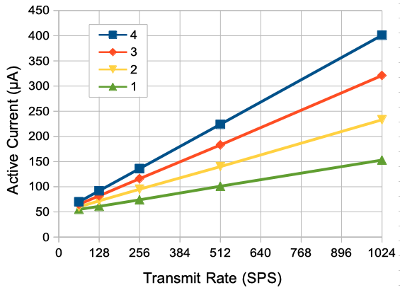
We take steps to reduce the length of the transmit interrupt by eliminating unecessary instructions. We replace our df_reg(0) flag on TP with CPUISRV, which somes directly from the CPU. Logic is 1178 LUTs. With TCK period 196-206 ns, our transmit interrupt is now 86 μs. Current consumption is 136 μA. We begin plotting current versus sample rate for various configurations. We have one to four inputs transmitting at sample rates 64 to 1024 SPS. The intercept of our plots is 48 μA, which is quiescent current of 33 μA plut 15 μA sampling current. The sampling current is constant because our V1.18 code does not skip sampling a channel when its period is set to zero. We could, in principle, reduce current consumption by around 4 μA per channel that is not in use. Our sampling cost is minimized when all four channels are running and share an interrupt, at which point we have 86 nA/SPS total.
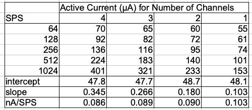
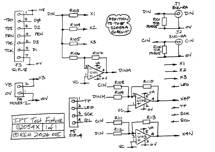
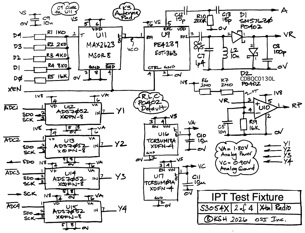
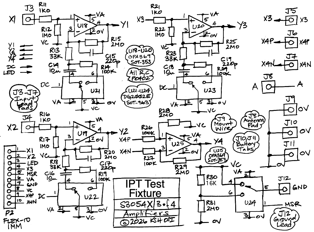
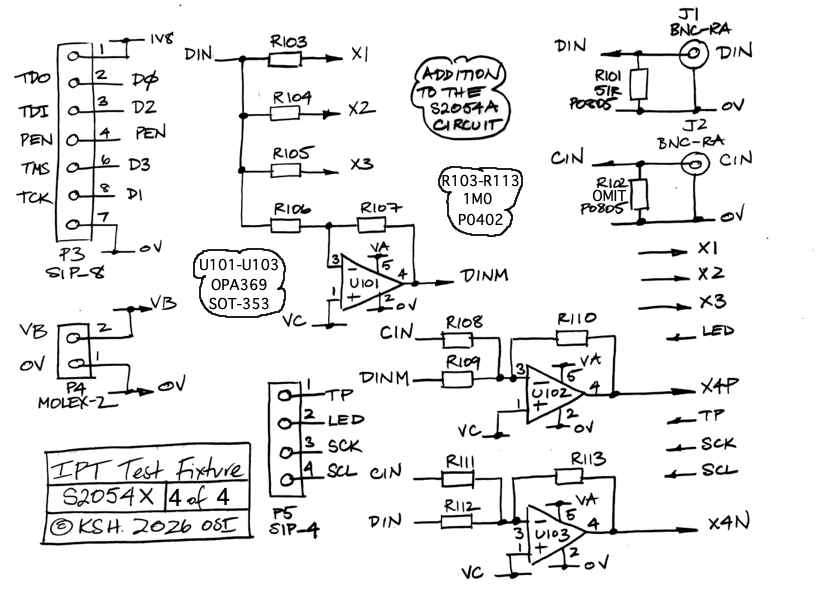
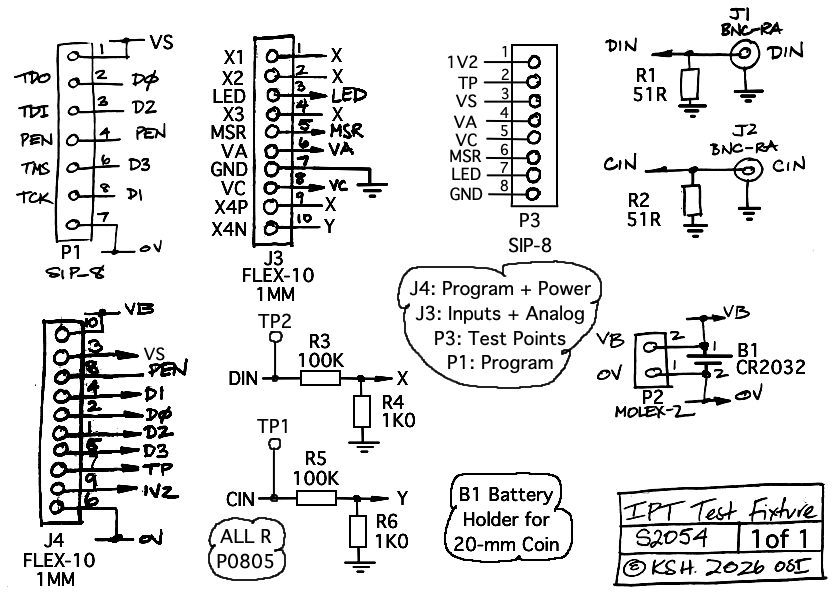
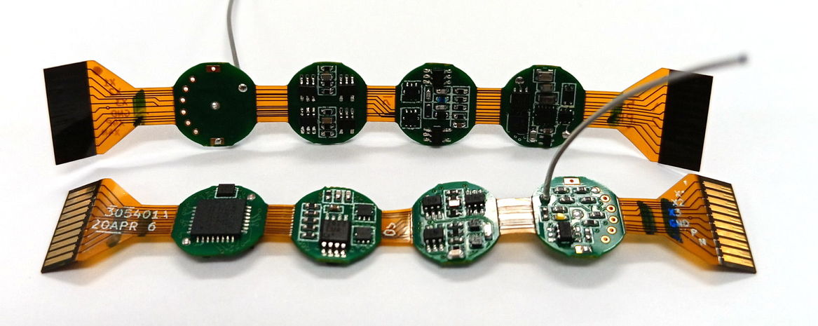